Table of Contents
The Critical Role of PCB Vias in Modern Electronic Design
In today’s high-density, high-performance electronic product designs, printed circuit board (PCB) vias serve as key elements for connecting multilayer circuits, with their importance becoming increasingly prominent. A skilled PCB design engineer must deeply understand the various characteristics of vias and their impact on circuit performance. This article provides a comprehensive analysis of the technical details of PCB vias, from basic concepts to advanced design techniques, helping you master this critical technical element.
Chapter 1: Basic Concepts and Core Functions of PCB Vias
1.1 Definition and Basic Structure of PCB Vias
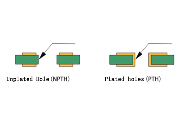
PCB vias, also known as plated through-holes, are conductive channels formed by drilling and copper-plating holes at the intersections of traces in multilayer PCBs. This structure enables electrical connections between different circuit layers and serves as the foundation of modern high-density PCB design.
The basic structure of a via includes:
- Drilled hole: Created via mechanical or laser processes
- Copper plating: Conductive metal layer covering the hole wall, typically 18-25μm thick
- Pad: Annular copper area connecting the hole to traces
- Solder mask: Selectively applied protective layer
1.2 Five Core Functions of PCB Vias
- Electrical connection: Enables conduction between signal, power, or ground layers, solving trace crossover issues in single-layer routing
- Space optimization: Significantly increases routing density and reduces PCB size through vertical interconnects
- Thermal management: Provides effective heat conduction paths for high-power components
- Signal integrity management: Controls transmission characteristics of high-frequency signals
- Mechanical support: Enhances PCB structural stability, particularly in through-hole component mounting areas
Chapter 2: In-Depth Analysis of PCB Via Types
2.1 Traditional Via Types
2.1.1 Through-Hole Via
- Structural features: Penetrates the entire PCB
- Advantages: Simple process, low cost, high reliability
- Disadvantages: Occupies more space, reduces routing density
- Typical applications: Standard multilayer boards, power connections
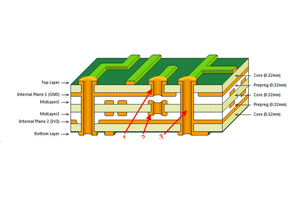
2.1.2 Blind Via
- Structural features: Connects outer layers to specific inner layers without penetrating the entire board
- Advantages: Saves space, increases routing flexibility
- Disadvantages: Requires laser drilling, higher cost
- Typical applications: Under BGA packages, high-density areas
2.1.3 Buried Via
- Structural features: Located entirely between inner layers, not exposed on surfaces
- Advantages: Maximizes outer layer routing space
- Disadvantages: Complex manufacturing process, difficult to repair or inspect
- Typical applications: High-layer-count PCBs, complex digital systems
2.2 Advanced Via Technologies
2.2.1 Micro Via
- Definition: Vias with diameters ≤0.15mm
- Manufacturing process: Laser drilling technology
- Advantages: Extremely small size, ultra-high density
- Applications: HDI boards, smartphone motherboards
2.2.2 Back Drilling
- Technical principle: Secondary drilling removes excess copper barrel
- Core value: Reduces stub effects, improves high-speed signal quality
- Typical applications: High-speed differential signals above 10 Gbps
2.2.3 Stacked Vias and Staggered Vias
- Stacked vias: Multiple micro vias vertically aligned
- Staggered vias: Offset micro via structures
- Performance comparison: Stacked vias save space but have lower reliability; staggered vias are the opposite
Chapter 3: Key Design Parameters and Optimization Strategies for PCB Vias
3.1 Via Size Specifications and Selection
3.1.1 Hole Size Selection
- Mechanical drilling limits: Typically ≥0.2mm
- Laser drilling capabilities: Can achieve 0.05-0.1mm
- Design recommendations:
- General signals: 0.3-0.5mm
- High-density areas: 0.15-0.2mm
- Power vias: ≥0.5mm (based on current requirements)
3.1.2 Pad Size Design
- Basic rule: Outer diameter = inner diameter + 0.2mm (minimum)
- High-density optimization: Use teardrop pads to enhance reliability
3.2 Electrical Characteristics Analysis of Vias
3.2.1 Parasitic Parameter Calculations
- Parasitic inductance: L≈5.08hln(4h/d)+1
- h: Via length (mm)
- d: Via diameter (mm)
- Parasitic capacitance: C≈1.41εrTD1/(D2-D1) (pF)
- εr: Dielectric constant
- T: Board thickness (mm)
- D1: Pad diameter (mm)
- D2: Anti-pad diameter (mm)
3.2.2 Impedance Control Techniques
- Anti-pad design: Increase spacing between vias and plane layers
- Ground via accompaniment: Place ground vias around signal vias
- Differential vias: Maintain symmetrical layout to minimize common-mode noise
3.3 Thermal Management Via Design
3.3.1 Thermal Via Array Design
- Layout principles: Evenly distribute under heat sources
- Size optimization: Diameter 0.3-0.5mm, spacing 1-2mm
- Fill materials: Thermally conductive epoxy or metal fill
3.3.2 Thermal Resistance Calculation and Optimization
- Single via thermal resistance: Rth≈h/(kπr²)
- h: Via length
- k: Copper thermal conductivity
- r: Via radius
- Array effect: Multiple parallel vias significantly reduce total thermal resistance
Chapter 4: Detailed PCB Via Processing Technologies
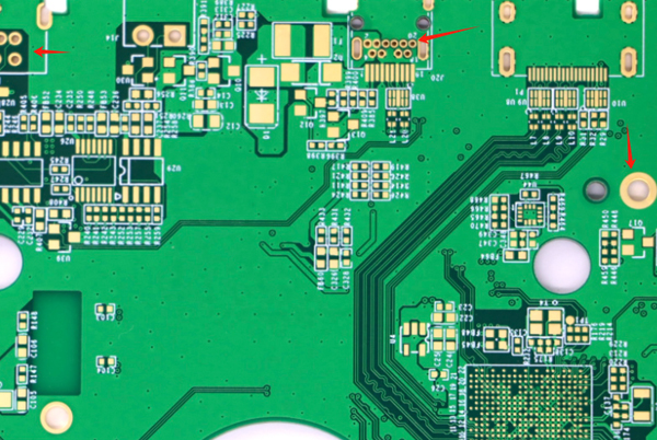
4.1 Comparison of the Four Main Treatment Methods
| Treatment Method | Process Characteristics | Advantages | Disadvantages | Typical Applications |
|---|---|---|---|---|
| Via Opening | No solder mask coverage on the surface | Good heat dissipation, testable | Prone to oxidation/shorts | Test points, thermal vias |
| Via Tenting | Surface covered with solder mask | Prevents shorts, low cost | Potential false copper exposure | Standard PCBs |
| Via Plugging | Filled with ink internally | High reliability | Hole size limit ≤0.5mm | High-quality PCBs |
| Resin Filling | Filled with resin | No oil leakage issues | Higher cost | HDI boards, high-frequency circuits |
4.2 Process Selection Guidelines
- Cost-sensitive projects: Prioritize via tenting
- High-reliability requirements: Use via plugging or resin filling
- High-frequency/high-speed designs: Must use resin filling to reduce parasitic effects
- Thermally critical areas: Select via opening with surface plating
4.3 Manufacturing File Annotation Standards
- Gerber files: Specify treatment requirements for each via type
- Drill drawings: Distinguish different hole sizes and via types
- Special notes: Indicate fill materials, surface treatments, etc.
Chapter 5: Practical PCB Via Design Techniques
5.1 High-Speed PCB Via Design Essentials
- Minimize stub length: Prefer blind vias or back drilling
- Ground via accompaniment: Place ground vias around signal vias (1:4 ratio)
- Anti-pad optimization: Control coupling capacitance between vias and planes
- Differential pair handling: Maintain symmetry to avoid phase deviation
5.2 Power Integrity Design Techniques
- Power via arrays: Provide low-impedance power paths
- Capacitor via optimization: Place vias close to decoupling capacitors
- Plane segmentation strategy: Avoid vias disrupting complete current return paths
5.3 High-Density Interconnect (HDI) Design Methods
- Micro via applications: Enable ultra-high-density routing
- Any-layer interconnects: Use stacked micro via technology
- Design rules: Follow 3-3-3 or 2-2-2 rules (layers-vias-traces)
5.4 Common Design Mistakes and Solutions
- Via bottlenecks: Insufficient power vias causing excessive voltage drop
- Solution: Perform current density simulation, increase via count
- Antenna effects: Isolated vias becoming radiation sources
- Solution: Ensure all vias have clear return paths
- Manufacturing defects: Via cracks or incomplete plating
- Solution: Follow the manufacturer’s aspect ratio recommendations (typically <8:1)
Chapter 6: Future Trends in PCB Via Design
6.1 Emerging Via Technologies
- Through-Silicon Vias (TSV): For advanced packaging
- Optical vias: Optical signal transmission in photonic integration
- Flexible vias: Interconnect solutions for bendable circuits
6.2 Evolution of Design Methodologies
- AI-assisted via optimization: Machine learning algorithms automate via placement
- Co-simulation platforms: Multi-physics EM-thermal-mechanical simulations
- DFM-integrated design: Real-time manufacturing constraint feedback
6.3 Industry Challenges and Solutions
- High-frequency loss issues: Application of new low-loss materials
- Miniaturization limits: Development of nano-scale drilling technologies
- Cost pressures: Hybrid via strategies for cost-performance optimization
Conclusion: The Art and Science of PCB Via Design
PCB via design is a professional field in electronic engineering that combines art and science. Excellent via design requires achieving the perfect balance between electrical performance, thermal management, mechanical reliability, and manufacturing costs. As electronic devices continue evolving toward higher frequencies and densities, via technologies will keep advancing, presenting engineers with new challenges and opportunities. Mastering the principles and techniques discussed in this article will help you design PCB products with outstanding performance and reliability.