Table of Contents
The Importance of Power Layers
In modern electronic devices, PCB power layers have evolved from simple power supply networks into critical factors that significantly impact system performance, stability, and reliability. Excellent power layer design not only ensures efficient power transmission but also significantly improves signal integrity, thermal management, and electromagnetic compatibility.
Basic Concepts of PCB Power Layers
What is a Power Layer?
A PCB power layer is a large-area copper foil layer specifically used for power distribution, usually located in the inner layers of multilayer PCBs. Compared to traditional power traces, power layers provide:
- Very low impedance paths: Reduce voltage drop and power loss
- Distributed capacitance: Form natural decoupling networks with ground layers
- Heat conduction paths: Effectively dissipate heat generated by components
Synergistic Effects Between Power and Ground Layers
Typical 4-layer board structure:
┌─────────────────────┐
│      Signal Layer   │
├─────────────────────┤
│      Ground Layer   │
├─────────────────────┤
│      Power Layer    │
├─────────────────────┤
│      Signal Layer   │
└─────────────────────┘

Power Layer-Ground Layer Capacitance Effect:
Power layers and adjacent ground layers form distributed capacitance,
providing high-frequency noise filtering function, effectively improving power quality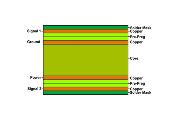
Core Technical Advantages of Power Layers
1. Power Integrity Optimization
- Reduced power impedance: Large copper areas provide milliohm-level impedance
- Improved transient response: Distributed capacitance provides rapid charge replenishment
- Reduced voltage fluctuations: Stabilize supply voltage, improve system reliability
2. Enhanced Signal Integrity
- Provide stable reference planes: Provide complete return paths for high-speed signals
- Reduce crosstalk: Isolate interference between different signal layers
- Impedance control: Maintain consistent transmission line characteristic impedance
3. Improved Thermal Management Performance
Heat conduction path analysis:
Heating components → Thermal vias → Power layer → Large-area heat dissipation- Uniform heat distribution: Copper layers quickly conduct and dissipate heat
- Reduced thermal resistance: Provide efficient thermal paths to heat sinks
- Prevent local overheating: Avoid reliability issues caused by heat concentration
4. Electromagnetic Compatibility (EMC) Improvement
- Reduce radiated emissions: Control current loop area
- Enhanced anti-interference capability: Provide shielding and filtering functions
- Meet regulatory requirements: Help pass EMC certification tests
Detailed Power Layer Design Practices
Stackup Strategy and Layer Design
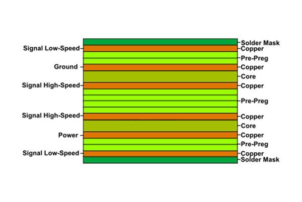
Comparison of Common Stackup Schemes
| Layers | Recommended Stackup | Application Scenarios | Advantages | Disadvantages |
|---|---|---|---|---|
| 4-layer | SIG-GND-PWR-SIG | General applications | Balanced cost, good performance | Limited power noise suppression |
| 6-layer | SIG-GND-SIG-PWR-GND-SIG | High-speed design | Excellent SI performance | Higher cost |
| | | SIG-GND-SIG-PWR-SIG-GND | Mixed-signal | Good isolation | High routing complexity |
| 8-layer | SIG-GND-SIG-PWR-GND-SIG-PWR-SIG | High-performance systems | Optimal performance | Highest cost |
Power Segmentation Techniques
Segmentation Principles and Methods
Power segmentation example:
+--------------------------------------------------+
|              Power Layer Segmentation Design     |
|                                                  |
|  +----------------+  +----------------------+    |
|  |   Digital 3.3V |  |      Analog 5V       |    |
|  |                |  |                      |    |
|  +----------------+  +----------------------+    |
|  |                 1.8V                     |    |
|  +------------------------------------------+    |
|  |              Core Voltage 0.9V           |    |
|  +------------------------------------------+    |
|                                                  |
+--------------------------------------------------+

Segmentation considerations:
1. Maintain proper spacing (typically 3-5 times dielectric thickness)
2. Avoid sensitive signals crossing segmentation areas
3. Provide sufficient decoupling for each region
4. Consider current capacity and thermal expansion coefficient
Via Design Specifications
Power Via Configuration Guidelines
- Current capacity calculation: Use IPC-2152 standard to calculate via size
- Array layout: Use a grid arrangement to optimize the current distribution
- Thermal management considerations: Add thermal vias for heat dissipation
- Impedance control: Maintain consistent via characteristic impedance
Power Layer Design for Mixed-Signal Systems
Digital-Analog Power Isolation Strategies
Mixed-signal power architecture:
┌──────────────────────────────────────────────┐
│            Power Layer Design Scheme         │
│                                              │
│  Digital Region      │      Analog Region    │
│  ┌─────────────┐     │  ┌──────────────────┐ │
│  │ Digital PWR │     │  │   Analog PWR     │ │
│  │   (1.2V)    │     │  │     (3.3V)       │ │
│  └─────────────┘     │  └──────────────────┘ │
│                      │                       │
│  Star connection point        Filter         │
│      └────────────┴─────────────┘            │
│               Isolation boundary             │
└──────────────────────────────────────────────┘
Split Ground and Power Management
- Digital noise isolation: Prevent switching noise from affecting analog circuits
- Proper connection points: Single-point connection at appropriate locations
- Filtering measures: Add π-filters at power entry points
- Return path management: Ensure complete current return paths
Power Layer Considerations in High-Frequency Design
Transmission Line Effect Management
- Wave propagation control: Maintain consistent characteristic impedance
- Resonance suppression: Use appropriate decoupling capacitor combinations
- Dielectric material selection: Choose low-loss factor materials
Power Distribution Network (PDN) Impedance Optimization
PDN impedance curve optimization:
Target impedance ────────────────
         │             │
         │  ┌─────────┴─┐
         │  │ Decoupling│
         │  │ Cap Effect│
         └──┴───────────┘
Frequency(Hz)- Low-frequency decoupling: Large electrolytic capacitors
- Mid-frequency decoupling: Ceramic capacitor arrays
- High-frequency decoupling: Embedded capacitor technology
Collaborative Design of Thermal Management and Power Layers
Thermal Performance Optimization Strategies
- Thermal via arrays: Arrange thermal vias under heating components
- Copper thickness selection: Choose an appropriate copper thickness based on current and heat dissipation requirements
- Heat spread design: Utilize power layers for uniform heat distribution
- Material matching: Select materials with appropriate thermal expansion coefficients
Current-Thermal Relationship Management
Thermal management calculation model:
Power loss(P) = I² × R
Temperature rise(ΔT) = P × θJA

Where:
I: Operating current
R: Power layer resistance
θJA: Junction-to-ambient thermal resistance

Reduce R and θJA by increasing copper thickness, expanding area, adding vias, etc.
Control temperature rise within safe limits
Advanced Power Layer Technologies
Embedded Component Technology
- Buried capacitance: Provides ultimate high-frequency decoupling
- Embedded power devices: Reduce parasitic parameters
- 3D integration: Achieve higher density power distribution
New Material Applications
- Low-loss substrates: Improve high-frequency performance
- High thermal conductivity materials: Enhance heat dissipation capability
- Flexible materials: Adapt to special application scenarios
Design Verification and Testing
Simulation Analysis Items
- DC drop analysis: Ensure voltage meets requirements
- Thermal analysis: Predict temperature distribution and hot spots
- Power integrity analysis: Verify PDN impedance
- Signal integrity analysis: Evaluate transmission quality
Physical Measurement Methods
- Network analyzer testing: Measure impedance characteristics
- Thermal imaging detection: Actual operating temperature distribution
- Noise measurement: Verify power quality
- Load testing: Assess transient response capability
Design Checklist
Key Points for Power Layer Design Verification
- Current capacity meets peak demand
- Voltage drop within the allowable range
- Proper decoupling capacitor placement
- Segmentation boundaries avoid sensitive signals
- Appropriate in quantity and size
- Thermal design meets temperature rise requirements
- Complete and effective EMC measures
- Feasible manufacturing process
Future Development Trends
Technology Development Directions
- Higher frequency support: Meet 5G/6G communication requirements
- Higher power density: Adapt to chip technology development
- Intelligent power management: Integrate monitoring and adjustment functions
- Sustainable design: Improve energy efficiency and environmental friendliness
Material Innovation Directions
- Nanomaterial applications: Improve electrical and thermal conductivity
- Biodegradable substrates: Environmentally friendly solutions
- Adaptive materials: Adjust characteristics based on conditions
Conclusions and Recommendations
PCB power layer design is a complex interdisciplinary engineering task that requires comprehensive consideration of electrical performance, thermal management, mechanical structure, and manufacturing processes. Successful power layer design should:
- System-level planning: Consider power architecture from project initiation
- Collaborative design: Optimize simultaneously with signal integrity and thermal management
- Simulation-driven: Identify problems in advance through simulation
- Physical verification: Confirm design effectiveness through testing
- Continuous improvement: Continuously optimize designs based on feedback
As electronic technology continues to develop, power layer design will evolve toward higher performance, increased integration, and enhanced intelligence, providing a reliable power foundation for next-generation electronic devices.