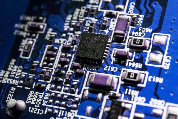
PCB electroplating is one of the core processes in printed circuit board manufacturing. It not only affects the appearance of the circuit but also plays a crucial role in enhancing electrical performance, improving the reliability of circuit connections, and facilitating efficient current transmission. Although often confused with surface treatment processes, electroplating serves distinct and well-defined functions in practical applications.
Table of Contents
What Is PCB Plating?
PCB plating refers to the chemical or electrochemical deposition of metals (typically copper) on the surface and through-holes of printed circuit boards. This process is primarily used to enhance electrical interconnections, improve current transmission capabilities, and protect circuits from environmental factors such as oxidation and moisture. Plating is not only crucial for the performance and reliability of circuit boards but also plays a key role in advanced applications like high-density interconnects (HDI) and high-frequency circuits.
Core Steps of PCB Plating
1. Electroless Copper Plating
Electroless copper plating is the foundational step of the plating process. It involves depositing a thin layer of copper on non-conductive substrates (such as hole walls and board surfaces) through autocatalytic reactions, providing a conductive base for subsequent plating. This step does not rely on external current but instead uses reducing agents to convert copper ions into metallic copper.
2. Board Preparation
- Hole Cleaning: Removes contaminants and resin residue left from drilling, ensuring strong plating adhesion.
- Micro-Etching: Slightly etches the copper surface to increase roughness and improve plating adhesion.
3. Pattern Transfer and Plating
- Use photoresist to cover areas not requiring plating, and form circuit patterns via UV exposure.
- Remove uncured photoresist to expose copper circuit areas to be plated.
- Plate copper and tin (as an etch-resistant layer) to thicken and protect the circuit patterns.
4. Post-Processing
- Remove photoresist and etch away non-circuit copper.
- Strip the tin layer to reveal the final copper circuit patterns.
Comparison of Main Plating Methods
| Method | Principle and Characteristics | Application Scenarios |
|---|---|---|
| Through-Hole Plating (PTH) | Deposits copper in holes via electroless and electrochemical plating to enable interlayer electrical connections | Multilayer boards, high-reliability electronic products |
| Finger Plating | Local plating of gold or rare metals to reduce contact resistance and enhance wear resistance | Gold fingers, edge connectors |
| Brush Plating | Uses anode-wrapped swabs to locally apply electrolyte for selective plating | Repairs and small-batch special area plating |
| Reel-to-Reel Selective Plating | Uses resist masks for patterned selective plating based on reel-to-reel processes | Flexible boards, connectors, IC pins |
Differences Between Electroplating and Electroless Plating
Although both methods are used for metal deposition, their principles and applications differ significantly:
- Electroplating: Relies on external current, offers fast deposition rates and controllable plating thickness, suitable for large-scale production.
- Electroless Plating: Achieves deposition through chemical reactions without external power, provides uniform plating, and is suitable for non-conductive substrates, but is slower and limited in thickness.
Surface Finishing: The Follow-Up Process to Plating
Surface finishing is a protective treatment applied to exposed copper surfaces after plating. Common methods include:
- Electroless Nickel Immersion Gold (ENIG): Provides a flat surface, high solderability, and oxidation resistance.
- Hot Air Solder Leveling (HASL): Low cost but poor surface flatness.
- Immersion Tin: Complies with Ro standards but may pose tin whisker risks.
Summary of the Importance of Plating
PCB plating is indispensable in modern electronics manufacturing. Its core values include:
- Enhancing electrical connections and signal transmission performance.
- Improving the mechanical strength and environmental adaptability of circuit boards.
- Providing a foundation for high-density interconnects and miniaturized designs.
- Ensuring soldering quality and extending product lifespan.