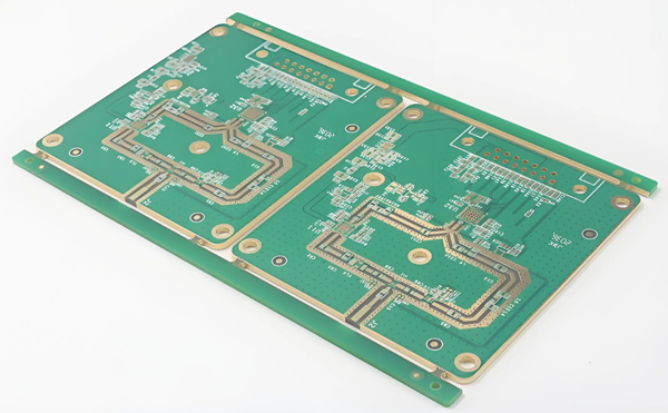
PCB (PrintedCircuitBoard), that is, printed circuit boards, is the core component of modern electronic equipment. PCB prototyping is the circuit design from the theory into the physical key steps. This article will introduce the basic process of PCB prototyping and the need to pay attention to the main points.
Table of Contents
PCB proofing before the need to do the preparatory work
- Physical border production
closed the physical border on the future layout of components, PCB proofing is a basic platform, must pay attention to the precise, and then is the corner of the place is best to use a rounded arc, not only to avoid being scratched by the sharp corners but also make the role of the stress can be mitigated. - The introduction of components and networks, and the layout of components
in the PCB prototyping components and networks lead to a good drawing of the border must be careful to operate according to the prompts, including the form of packaging components, and components network issues. PCB prototyping layout components and alignment of the product’s life, stability, and electromagnetic compatibility have a great impact and are the places where special attention should be paid. - PCB design and wiring and adjust the perfect
In the PCB design and wiring,g it is best to pay attention to the requirements of the processing parameters, or the trusted PCB prototyping manufacturers, the defective rate will be greatly reduced. After completing the PCB design and wiring, to do is to the text, individual components, and some adjustments to the alignment and copper (this work should not be too early, otherwise it will affect the speed, but also the PCB design and wiring to bring trouble), the same to facilitate production, debugging, maintenance. - Check the network
Sometimes because of misuse or negligence caused by the network relationship between the painted PCB board and the schematic diagram is different, then checking the check is very necessary. So painting should be done after checking, and then the follow-up work.
PCB production sampling process
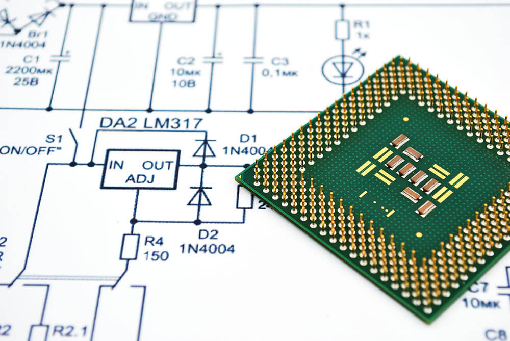
- Circuit design: the need to complete the circuit schematic design. This step is usually completed by electronic engineers using professional circuit design software.
- PCB drawing: After the circuit design is completed, it needs to be converted into PCB graphics. This process requires the use of professional PCB design software, such as AltiumDesigner, Eagle and so on. Drawing process needs to pay attention to the layout between the components, wiring and other details.
- PCB file output: After completing the PCB graphic design, you need to output the file for the PCB production manufacturers need the format, such as Gerber files. This step is usually completed directly by the design software.
- PCB production sampling: the output PCB files sent to PCB manufacturers, production sampling. The production process needs to pay attention to material selection, production process, production cycle, etc.
- PCB Inspection and Testing: After receiving the prototype, the PCB needs to be inspected and tested in detail to ensure that it meets the design requirements.
PCB Production Proofing Points
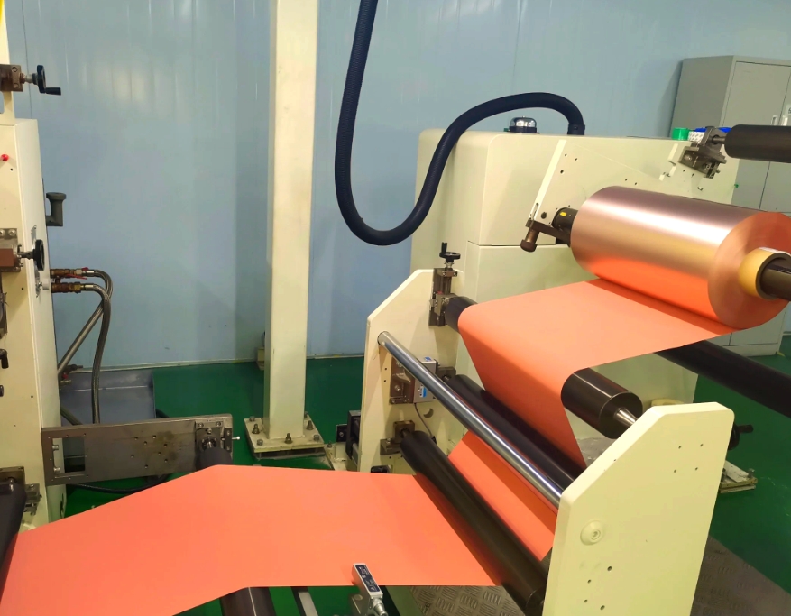
- Material Selection: The selection of materials for PCB production is very important, and common materials include FR4, CEM-1, aluminum substrate, and so on. The selection of the appropriate material needs to be based on the actual needs and application scenarios.
- Production process: The PCB production process includes etching, drilling, welding, and so on. Different production processes will have an impact on the quality and performance of the PCB. When choosing the production process, you need to weigh the actual needs.
- Production cycle: the production cycle of PCB prototyping varies depending on the manufacturer and the production process. When choosing a manufacturer, you need to pay attention to its production capacity and delivery time to ensure that the project is completed on time.
- File output and verification: Before outputting the PCB file, you need to carefully verify the correctness of the circuit design and PCB graphics. Communicate with PCB manufacturers to confirm the file format and requirements to avoid compatibility problems.
- Communication and feedback: In the process of communication with PCB manufacturers, you need to clearly express their needs and requirements. After receiving the prototype, timely inspection and testing, found that the problem is timely communication with the manufacturer to solve.
PCB production sampling common problems and solutions
- PCB short circuit: this may be due to the unreasonable layout of components, wires being too thin, and other reasons. Solutions include optimizing the layout of components, thickening the line, and so on.
- PCB broken circuit: may be due to drilling deviation, poor welding and other reasons. Solutions include improving drilling accuracy, optimize the welding process.
- PCB size does not match: may be due to file output errors or manufacturers of production errors. Solutions include careful verification of documents, communicate with manufacturers to confirm the size requirements.
PCB Production Proofing Time
| PCB Layers | Quick Turnaround (Prototype) | Standard Production (Mass) |
|---|---|---|
| 2-layer | 12 hours | 8-10 business days |
| 4-layer | 24 hours | 10-12 business days |
| 6-layer | 48 hours | 12-14 business days |
| 8-layer | 72 hours | 16-18 business days |
| 10-layer | 72 hours | 18-20 business days |
| 12-layer | 96 hours | 18-20 business days |
PCB Fabrication Proofing Costs
The cost of proofing PCBs (printed circuit boards) is usually influenced by several factors, including design complexity, PCB size, number of layers, material selection, copper thickness, manufacturing process, and quantity. In general, the cost of prototyping a single-sided PCB is relatively low, while the cost of a multi-layer PCB can increase significantly.
Proofing a simple single-sided PCB is roughly around a few hundred RMB, and for a double-sided PCB, the price may range from 800 RMB to 2,000 RMB. For multilayer PCBs, especially designs with more than four or six layers, the cost can be even higher, sometimes reaching several thousand dollars. In addition, the type of material used (e.g., FR-4, aluminum substrate, etc.) and the surface treatment process (e.g., metal plating, lead-free process, etc.) will also affect the final cost.
The number of proofs is also an important factor in determining cost. Some manufacturers often have additional costs when offering small quantities for sampling, so it is recommended to try to anticipate future production quantities when finalizing the design. If more than one PCB is sampled at a time, the unit cost may go down.
What are the PCB proofing precautions?
PCB proofing precautions mainly include the following aspects
Design phase: In the design phase, you need to fully consider the limitations and constraints of the actual production, such as board size, component packaging, etc.. Follow the relevant standards and specifications to ensure the rationality and reliability of the design
Document preparation: In the document preparation process, you need to carefully check the design documents and BOM files to ensure the accuracy and completeness of the documents. Pay attention to file format and compatibility to avoid sampling failure or delay due to file problems
Selecting a Proofing Manufacturer: Selecting the right PCB proofing manufacturer is the key to ensuring the quality of proofing. You need to consider the manufacturer’s production capacity, equipment level, and quality visibility. You can check the manufacturer’s history, customer reviews, and other ways to understand its reputation and quality of service
Proofing production: In the proofing production process, the manufacturer will be following the design requirements of strict quality control to ensure that the quality of the proofing board meets the requirements. Customers receive the prototype board but also need to carry out quality acceptance, to ensure that the prototype board is in line with the design requirements and the use of demand
Tests and modifications: After the completion of the prototype, the board needs to be tested to verify that its function and performance are in line with the design requirements. If problems are found during testing, modifications, and optimization need to be made based on the test results, and then re-proofing and testing
Cost Control: Cost control factors should be taken into account when prototyping PCBs. Choose the right PCB manufacturer, and optimize the design to reduce material and process costs.
Summarize: PCB production sampling is an indispensable part of the development process of electronic products. In practice, you need to pay attention to the material selection, production process, production cycle, and other key points, and PCB manufacturers to maintain good communication and feedback. Only in this way can ensure the smooth progress of PCB prototyping, laying a solid foundation for the successful development of electronic products.