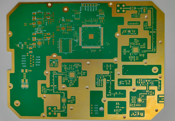
PCB is an integral part of electronic equipment, which makes the electronic components in the circuit can be connected to each other to form a complete circuit system.PCB design and production process involves a number of links, requiring specialized skills and knowledge.
Table of Contents
First, the design stage
- Schematic design: engineers use professional circuit design software, such as AltiumDesigner, EAGLE, etc., to draw circuit schematics. This stage needs to ensure that the logic and function of the circuit are correct.
- PCB layout and wiring: After the schematic verification is correct, the engineer will carry out the PCB layout and wiring design. This stage needs to take into account factors such as electrical connections between components, signal transmission, heat dissipation, and mechanical strength.
- Design review and optimization: After completing the preliminary design, a design review is required to ensure that the design meets the production requirements. If problems are found, it needs to be optimized and adjusted in time.
Second, the production stage
- Production of film: the designed PCB pattern is converted to the actual production of the actual graphics required. This step is usually completed by a professional film production company.
- Production of copper plate: the film and copper plate for exposure, development, etching, and other processes to produce a copper plate with circuit graphics.
- Drilling and milling: According to the design requirements, drilling holes in the copper plate, in order to install components and welding. Milling the edges of the copper plate as needed to form the desired shape and size.
- Surface treatment: according to the need, the copper plate surface treatment, such as spraying tin, immersion gold, etc., in order to increase the conductivity and corrosion resistance.
- Inspection and testing: Strict inspection and testing of the finished PCB boards to ensure that their electrical and mechanical properties meet the design requirements.
Third, the production stage
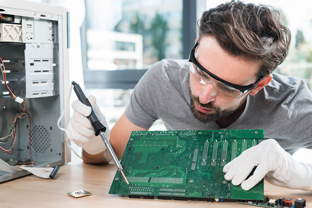
- SMT placement: Use automatic placement machines to accurately attach surface mount components (such as resistors, capacitors, ICs, etc.) to the PCB board.
- Wave soldering and manual soldering: For components that need to be connected by soldering, use a wave soldering machine or manual soldering station.
- Cleaning and inspection: After soldering is completed, the PCB board is cleaned to remove flux and other residues. Then the appearance and electrical properties of the inspection to ensure the quality of welding.
- Assembly and testing: The PCB board is assembled with other components, and then the overall function is tested. This step usually includes a power-on test, signal test, and so on.
- Aging and Screening: Aging the products that pass the test to detect their stability and reliability. At the same time, screening is carried out to eliminate unqualified products.
- Packaging and shipping: Qualified products are packaged and then shipped according to customer requirements. Packaging usually has anti-static bags, upper and lower tape, release film ,and so on.
Fourth, quality control and continuous improvement
In the whole production process, quality control is a crucial part. The factory needs to establish a strict quality management system to strictly control each link to ensure the quality and performance of the final product. Through the collection of customer feedback and market information, the production process can be continuously improved and optimized to increase the competitiveness and market share of the products. The production process of PCB boards is a complex and precise process, which requires strict control of each link to ensure the quality and performance of the final products. With the continuous development of science and technology, PCB board production technology is also progressing, providing strong support for the rapid development of the electronics industry.
Etching film production is a common method of making printed circuit boards, and its process is to strip the part to be etched by chemical reaction, so as to form the pattern of the circuit board.
1. Preparation
Before making etching film, you need to prepare the following materials and tools:
- etching solution: generally used is ferric chloride or hydrogen peroxide.
- FILM PAPER: Used to print the circuit board pattern.
- Photopolymer: an important material for transferring the circuit board pattern to the copper plate.
- photosensitive board: a special type of copper board coated with photosensitive adhesive.
- UV Lamp: Used to expose the photosensitive board.
- Etching machine: Used to etch off the excess copper on the copper plate.
- plate washer: used to clean the photosensitive plate and the etched copper plate.
2. Production Steps
- Printing Patterns
After making the pattern of the circuit board to be produced, use the printer to print the pattern on the film paper. - Prepare the photosensitive board
Put the photosensitive board into a dark environment, take out one photosensitive board, coat it with photosensitive adhesive, and then dry it with a hot air gun. - Exposure
Place the printed film sheet on the photosensitive plate and place it under a UV lamp for exposure.
The exposure time depends on the type of photopolymer and the power of the UV lamp and usually takes a few minutes to ten minutes. - development
will be exposed to the photosensitive plate in the development solution, the unexposed photopolymer will be dissolved to reveal the surface of the copper plate.
Developing time is generally a few minutes. - etching
will be developed after the copper plate into the etching solution, the copper is not protected by the photopolymer etching off.
The type and concentration of the etching solution depends on the material to be etched and the pattern, which generally takes a few minutes to half an hour. 6. - Cleaning
Place the etched copper plate into the plate washer to clean off the excess etchant and photopolymer.
During the cleaning process, care should be taken to protect your skin and eyes from contact with the etchant.
3. Precautions
- The environment should be kept clean and tidy during the production process to avoid dust and impurities contaminating the photosensitive board and copper plate.
2, in the exposure, development, and etching process, should pay attention to protecting their skin and eyes, and avoid contact with chemical liquids. - When choosing etching and developing solutions, different types and concentrations of liquids should be selected according to actual needs.
- When etching, you should choose the appropriate etching time and concentration according to the complexity of the pattern and the required precision.