Table of Contents
What is PCB Panelization?
PCB panelization is a manufacturing process that involves designing multiple identical or different single PCBs on the same substrate to form an integrated processing unit. Just like a cookie cutter stamps multiple cookies at once, PCB panelization allows manufacturers to complete multiple single boards simultaneously through a single process, like exposure, etching, and drilling.
Three Core Values of PCB Panelization
Improved Production Efficiency: Taking smartphone motherboards (approximately 100mm×60mm) as an example, panelizing them into a 400mm×300mm standard board allows processing 20 single boards at once, increasing production efficiency by 18 times.
Reduced Production Costs: With panelization, equipment utilization in SMT assembly lines can increase from 60% to 85%, reducing processing costs per PCB by 22%.
Enhanced Product Quality: Panelized boards have increased overall rigidity, improving dimensional stability by over 30% and controlling circuit precision deviation within ±3μm.
Three Main Methods of PCB Panelization
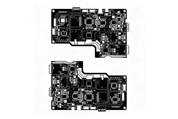
1. V-CUT Panelization Method
V-CUT is the most common panelization method, particularly suitable for regular rectangular PCBs:
- Working Principle: V-shaped blades cut shallow grooves between adjacent boards (depth approximately 1/3 of board thickness), leaving minimal material connection.
- Applicable Scenarios: Regular rectangular boards with straight connecting edges.
- Technical Parameters:
- V-shaped angle, typically 45°
- Remaining thickness should be 1/4-1/3 of board thickness, and ≥0.4mm
- Copper traces/wires should be ≥0.4mm from the V-CUT centerline.
- Advantages: Easy separation, low cost, clean appearance.
- Limitations: Only suitable for straight lines; insufficient strength when board thickness <1.0mm.
2. Tab-Routing Panelization Method
Tab-routing (also known as breakaway tab or mouse bites) is suitable for irregular boards or complex separation paths:
- Working Principle: Boards are connected through multiple small holes (small round holes + short connections) between boards.
- Applicable Scenarios: Irregular boards, circular boards, or non-linear edges.
- Technical Parameters:
- Hole diameter: 0.55mm
- Hole spacing: 0.2mm
- Hole center distance: 0.75mm
- Distance between adjacent holes in the same row: 1mm
- Distance between two rows of holes: 2mm
- Design Points:
- Tabs should extend 1/3 into the board.
- After adding tab holes, connect outlines on both sides using a keep-out layer.
- Typically, use 2-3 connecting tabs.
- Advantages: High flexibility, adaptable to various shapes.
- Disadvantages: Burrs after separation may require post-processing.
3. Hollow Tab Panelization Method
Hollow tabs are an improved form of tab routing, mainly used for special scenarios:
- Working Principle: Connection via narrow board material without through-holes.
- Applicable Scenarios: Special structures like modules with half-holes on all sides.
- Advantages: Higher connection strength than tab-routing.
- Disadvantages: Noticeable protrusions at connection points after separation.
Detailed PCB Panelization Process
Step 1: Tab-Routing Design
- Determine panelization connection method (based on board shape).
- Design tab-routing parameters:
- 8 holes of 0.55mm diameter.
- Hole spacing: 0.2mm.
- Hole center distance: 0.75mm.
- Ensure tabs extend 1/3 into the board.
- Use a keep-out layer to connect outlines on both sides of holes.
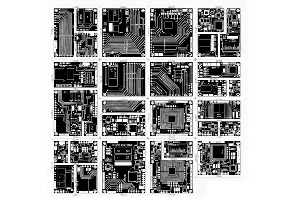
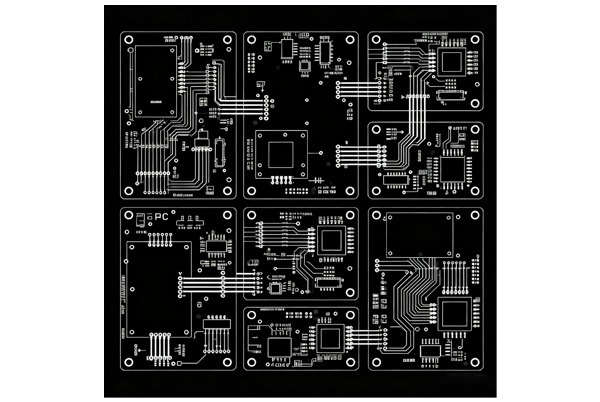
Step 2: Unit Layout
- Determine panelization quantity (e.g., 2×2, 3×3 matrix).
- Copy PCB units using the special paste function:
- Ctrl+A to select all, Ctrl+C to copy.
- Use “Paste Special” to ensure network names are preserved.
- Adjust unit positions to ensure consistent orientation.
- Remove unnecessary connection structures.
Step 3: Process Edge Design and Optimization
Process edges are used for machine feeding during SMT assembly:
- Width Requirements: Standard 5mm (minimum 3mm).
- Tooling Holes: 4 non-plated holes of 2mm diameter.
- Fiducial Marks: 1mm diameter solder pads with HASL finish.
- Layout Rules:
- No components on process edges.
- Fiducial marks in L-shaped distribution, diagonally asymmetric.
- Fiducial mark edges are at least 3.5mm from the board edge.
Key Considerations for PCB Panelization
Dimension and Shape Specifications
- Equipment Limitations:
- SIEMENS line: Panel width ≤260mm.
- FUJI line: Panel width ≤300mm.
- Automatic dispensing: Panel size ≤125mm×180mm.
- Panel Dimensions:
- Optimal size: Approximately 150mm×200mm.
- Minimum single board: Not less than 50mm×50mm.
- Board utilization: Should reach 85% or above.
Component Layout Essentials
- Clearance: Components ≥0.5mm from board edge.
- Large Component Fixation: Large components like I/O interfaces need locating posts or holes.
- Connector Placement: Away from panelization connection points.
- Uniform Orientation: All single boards maintain the same placement direction.
Positioning System Design
- Tooling Holes:
- At least three per small board, 3-6mm diameter.
- No traces within 1mm of edge tooling holes.
- Four 4mm±0.01mm tooling holes at panel corners.
- Fiducial Marks:
- 1mm diameter solid circles, copper with HASL.
- 1.5mm clearance around marks without solder mask.
- ≥5mm distance from other metal points.
PCB Panelization Optimization Strategies
Efficiency Optimization Techniques
- Compact Layout: Spacing reduced from 0.8mm to 0.5mm, process edges from 5mm to 3mm.
- Modular Panelization: Different versions of the same project combined, reducing the prototyping cycle by 2 days.
- Nested Layout: Irregular and standard boards nested together, improving material utilization by 19%.
Quality Improvement Methods
- Stress Control: V-CUT separation along a straight direction, avoiding lateral bending.
- Connection Optimization: ≤3 tab-routing connection points to reduce separation stress.
- Thermal Management: Pre-heat treatment (60℃×10min) before separation to reduce board brittleness.
Cost Control Strategies
- Material Optimization: Intelligent nested layout improves utilization from 58% to 92%.
- Process Combination: “V-CUT pre-cutting + tab-routing” combination improves separation efficiency 3 times.
- Standardization: Establish a panel size system to reduce special processing requirements.
Common Issues and Solutions
| Issue Type | Manifestation | Solution |
|---|---|---|
| Panel Warping | Bending due to improper storage | Use a closed-frame design, reducing warpage by 83% |
| Solder Bridging | Caused by excessive center distance | Control center distance between 75-145mm |
| Placement Offset | Missing fiducial marks | Ensure sufficient fiducial marks per board |
| Component Damage | Fracture near the board edge | Maintain ≥0.5mm distance between components and board edge |
Recommended Professional Tools
- Huaqiu DFM: Panel utilization calculation, automatic layout optimization.
- Altium Designer: Embedded Board Array function for direct panelization.
- VayoExpert Panel Designer: Intelligent board outline recognition, automatic conflict avoidance.
Conclusion
PCB panelization is a critical link between design and manufacturing. Proper panel design can significantly improve production efficiency, reduce costs, and ensure quality. When selecting panelization methods, comprehensively consider board shape, batch size, cost, and quality requirements, follow design specifications, and fully utilize professional tools to achieve optimal panelization results.
By implementing scientific panelization strategies, companies can achieve remarkable benefits: 18x production efficiency improvement, 22% cost reduction, and 30% quality stability enhancement.