Table of Contents
Advantages of PCB Panelization and Methods
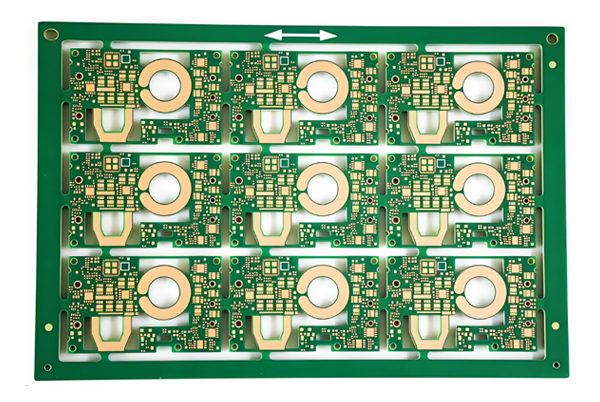
PCB panelization optimizes production by efficiently arranging multiple circuit board units on a single substrate (FR-4/Aluminum, etc.). Its key benefits include:
- Material utilization improved by 30%-50%
- SMT assembly efficiency increased by 40%
- Production costs reduced by 15%-25%
1.1 V-Scoring (V-CUT)
Best for: Rectangular boards (aspect ratio < 3:1)
Specifications:
- Cutting angle: 30°/45°, remaining thickness: 0.3±0.1mm
- Spacing requirement: ≥0.4mm between adjacent units (to prevent chipping)
- Design marking: Use 0.15mm line width in Keepout layer
Case Study: For 6-layer impedance boards, V-scoring must avoid internal power copper layers to prevent short circuits caused by burrs.
1.2 Breakaway Tab (Mouse Bite) Panelization
Solution for irregular boards:
- Hole diameter: 0.55mm (±0.05mm tolerance)
- Matrix layout: 8 holes/group, pitch: 0.75mm
- Extension depth: 1/3 of board thickness (to ensure clean breaks)
Design Guidelines:
- Place tabs in non-critical stress areas
- Ensure copper isolation in Keepout layer
1.3 Hollow Bridge Connections
For half-hole modules:
- Bridge width: 1.2mm (40% narrower than breakaway tabs)
- Must be placed at board corners (stress dispersion zones)
- Apply teardrops to prevent tearing
2. Standard Panelization Workflow (Breakaway Tabs Example)
2.1 Design Phase
- DFM Check: Confirm 3.5mm clearance from board edges
- Hole Array Layout: Generate 0.55mm via groups using array tools
- Copper Isolation: Draw isolation zones in Keepout layer
2.2 Panelization Execution
| Step | Requirements | Recommended Tools |
|---|---|---|
| Unit Replication | Spacing ≥2mm | Altium Multi-Channel Design |
| Process Edge Addition | 5mm + 3mm compensation | CAM350 Verification |
| Fiducial Marker Placement | L-shaped asymmetric layout | Script automation |
2.3 Output Verification
- Gerber Check: Ensure V-scoring and drill layer alignment <0.1mm
- Panel Simulation: Conduct stress analysis using Valor NPI
3. Common Issues & Solutions
Q1: Rough edges after breakaway tab separation?
A:
- Increase hole wall copper thickness from 35μm to 50μm
- Add laser etching (additional $0.02/board)
- Align break direction with PCB fiber grain
Q2: Uneven breaks after V-scoring?
A:
- Check tool wear (replace after every 500 cuts)
- Adjust cutting depth to 1/3 of board thickness
- For high-frequency boards, switch to laser V-scoring
Q3: Fiducial markers on process edges obstructed?
A:
- Increase anti-pad diameter to 2mm
- Add recognition symbols (Ⓜ) in stencil layer
- Use tri-color fiducials (copper base/white ring/black core)
4. Advanced Optimization Tips
- Hybrid Panelization: Combine V-scoring and breakaway tabs for HDI boards (6+ layers)
- Dynamic Routing: Use CNC for automatic connector optimization
- Cost Calculation: Utilize tools like PCBCart’s panelization calculator
Scientific panelization can increase material utilization from 65% to 92% (per IPC-7351B standards). Implement MES systems for real-time efficiency monitoring.