
PCB design is a core aspect of electronic engineering, involving the conversion of circuit schematics into actual production-ready printed circuit board layouts, requiring comprehensive consideration of component layout, signal integrity, heat dissipation and electromagnetic compatibility.
Table of Contents
The basic process of PCB design
PCB design usually includes the following major steps:
- Demand analysis and planning
Engineers plan the basic modules of the circuit and draw the circuit diagram of the product according to the circuit site conditions, market research or product innovation needs.
Determine the circuit function, signal type (high speed, low frequency, RF, etc.).
Select the number of PCB layers (single, double or multilayer boards).
Determine dimensions, mounting methods, and mechanical constraints. - Schematic design
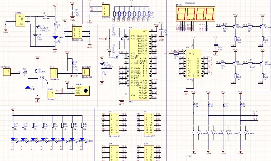
Draw specific schematic diagrams based on the product circuit framework diagram to materialize the circuit system.
Use EDA (Electronic Design Automation) tools (e.g. Altium Designer, KiCad, Cadence, etc.) to draw the circuit schematic.
Ensure that all components are correctly symbolized and connected.
Perform ERC (Electrical Rule Check) to avoid problems such as short circuits, open circuits, etc. - PCB Layout
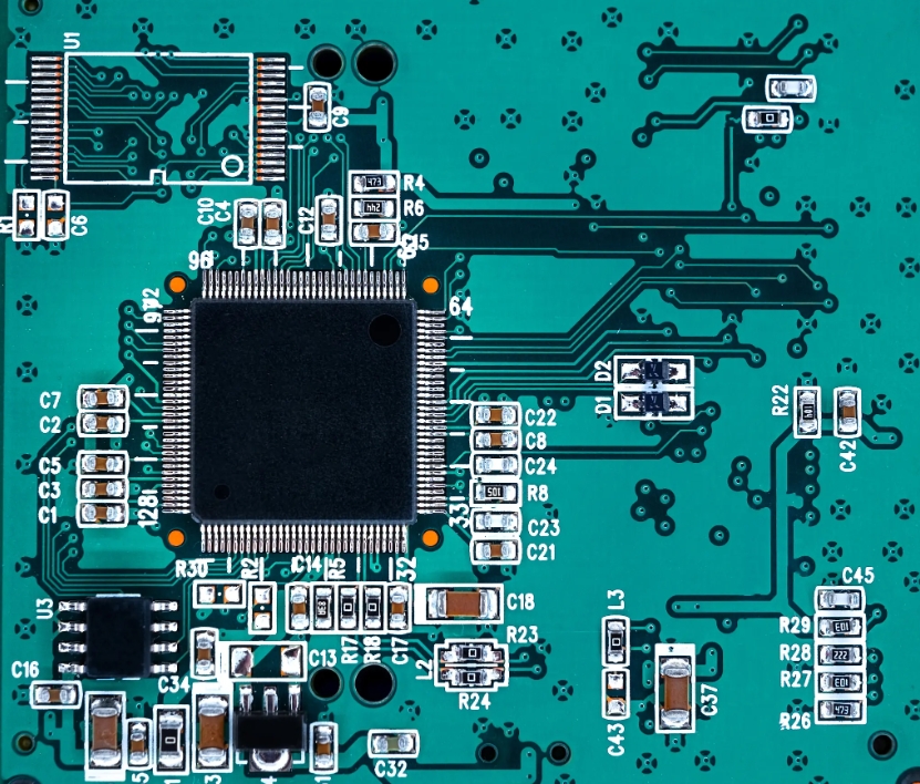
After drawing the schematic, you need to transfer the component package and component connection information to the PCB board design environment. After the component package is transferred to the pcb board design environment, you need to lay out the components according to the product’s chassis shape, panel structure, EMC specifications, reasonable requirements for electrical layout, and characteristics of the pcb board design stacked structure.
Components are placed on the PCB according to the schematic diagram, taking into account factors such as signal flow, heat dissipation, and electromagnetic compatibility (EMC).
Key components (e.g. MCU, crystal, power module) are prioritized for layout to shorten the critical signal path.
Partition layout: analog, digital, and power supply parts are separated to reduce interference. - PCB wiring
After the components are arranged, the pre-drawn lines generated according to the network table in the pcb board design are filled with solid lines, and the rationality of the circuit board wiring will directly affect the quality of the circuit board.
Power wiring: widen the power line, reduce impedance, avoid voltage drop.
Signal lines: high-speed signals (such as USB, HDMI) need to control the impedance, to avoid too long alignment.
Ground processing: using star grounding or laying copper to reduce noise. - DRC (Design Rule Check)
Check whether the wire width, spacing, and crossing holes meet the manufacturing requirements.
Confirm that there are no short circuits, broken circuits, unconnected networks, etc. - Output production files
Generate Gerber file (for PCB manufacturing).
Provide drill file (NC Drill) and BOM (Bill of Materials).
PCB design rules
1. in general, all the components should be arranged on the same surface of the circuit board, only the top layer of components is too dense, in order to be a number of highly limited and small heat devices, such as chip resistors, chip capacitors, chip ICs and so on in the bottom layer.
2. under the premise of ensuring electrical performance, components should be placed on the grid and parallel or perpendicular to each other, in order to neat, beautiful, in general, does not allow the components to overlap; components to be arranged in a compact, components in the entire layout should be evenly distributed, dense and consistent.
3. the minimum distance between the adjacent pad graphics of different components on the circuit board should be more than 1MM.
4. from the edge of the circuit board is generally not less than 2MM. the best shape of the circuit board for the rectangular, the length to width ratio of 3:2 or 4:3. circuit board surface footage is greater than 200MM by 150MM, should be considered when the circuit board can withstand the mechanical strength.
PCB design skills
In the PCB layout design to analyze the circuit board unit, based on the starting function of the layout design, the layout of all the components of the circuit, to comply with the following principles:
1.in accordance with the flow of the circuit to arrange the location of each functional circuit unit, so that the layout facilitates the flow of signals, and make the signals as far as possible to maintain a consistent direction.
2.Take the core component of each functional unit as the center and layout around him. Components should be uniform, integral, compact arrangement on the PCB, minimize and shorten the lead and connection between the components.
3.circuits operating at high frequencies, to consider the distribution parameters between components. General circuits should be as far as possible so that components are arranged in parallel, which is not only beautiful, but also easy to load and weld, easy to mass production.
Key Points for PCB Design
- Signal Integrity (SI)
High-speed signals need to consider impedance matching to avoid reflections and crosstalk.
Use differential pairs (e.g., USB, LVDS) and maintain equal alignment lengths. 2. - Power Integrity (PI)
Use decoupling capacitors (0.1μF near IC power pins).
Multilayer boards can use power planes to reduce noise. - Electromagnetic Compatibility (EMC)
Avoid sharp angle alignment to reduce high frequency radiation.
Keep critical signal lines away from clock and high frequency areas. - Thermal Management
High-current components (such as MOSFETs, LDOs) to increase the heat sink or heat sink.
Reasonable layout of heat generating components to avoid localized overheating. - Manufacturability (DFM)
Line width/spacing meets PCB manufacturer’s process capability (e.g., minimum 6 mil line width).
Avoid too small vias (e.g. below 0.3mm may increase cost).
Summarize
PCB design is an important part of electronic engineering. Good design can improve circuit stability, reduce noise and optimize production costs. Mastering the basic flow, focusing on signal integrity, power management and EMC, and verifying with the help of professional tools can significantly improve the quality of PCB design.