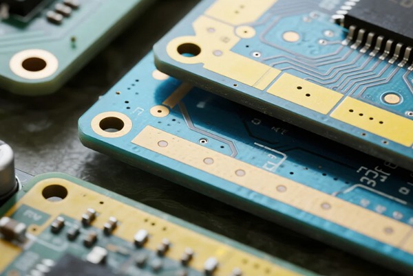
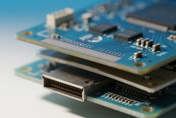
Printed circuit boards (PCBs) are the core carriers of electronic devices. The number of layers they have directly impacts how well the product works, how much it costs, and how reliable it is. This article will look at the theoretical limits of PCB layer counts, the practical things that make it difficult to manufacture them, how they compare when you look at the advantages and disadvantages of different layer counts, and the technical things to think about when choosing the right layer counts. It will provide a complete reference for electronic engineers and product designers.
Table of Contents
I. Theoretical Limits and Practical Manufacturing Constraints of PCB Layers
Theoretical Layer Limits
There is no absolute upper limit to the number of layers in a PCB. With advancements in microelectronics technology, leading global manufacturers like Intel and Samsung have achieved mass production of PCBs with 100+ layers, primarily for specialized applications such as supercomputers, high-end servers, and aerospace equipment.
Practical Manufacturing Constraints
Despite the theoretical possibility, practical mass production faces several limitations:
- Technical constraints: Layer-to-layer alignment precision requirements increase exponentially with added layers
- Material constraints: High-layer-count PCBs require highly stable materials with low thermal expansion coefficients
- Cost constraints: The manufacturing cost of a 32-layer PCB can be 5-8 times that of a 4-layer board
- Yield constraints: Beyond 20 layers, each additional layer reduces yield by approximately 2-3%
Standard Production Layer Ranges
The table below shows typical PCB layer distributions across different application fields:
| Application Field | Typical Layers | Representative Products | Technical Characteristics |
|---|---|---|---|
| Consumer Electronics | 4-8 layers | Smartphones, Tablets | Cost-sensitive, space-constrained |
| Communication Equipment | 8-16 layers | 5G Base Stations, Network Switches | High-frequency, high-speed, thermal management requirements |
| Industrial Control | 6-14 layers | PLCs, Industrial Motherboards | High reliability, strong interference immunity |
| High-end Computing | 12-32 layers | Servers, AI Accelerator Cards | Ultra-high density, high-speed transmission |
| Specialized Fields | 32-100+ layers | Supercomputers, Aerospace Equipment | Extreme performance, special materials |
II. Comprehensive Analysis of Multilayer PCB Advantages
1. High-Density Integration Capability
Through layered stacking design, multilayer PCBs significantly improve wiring density within limited areas. Test data shows that 8-layer boards provide approximately 60% higher wiring density than 4-layer boards, while 16-layer boards can improve density by over 120%.
2. Excellent Signal Integrity
Through proper stack-up design and impedance control, multilayer PCBs effectively ensure high-speed signal transmission quality:
- 4-layer boards: Reduce signal attenuation by over 40% compared to double-sided boards at 1GHz frequency
- 8-layer boards: Support high-speed interfaces like PCIe 4.0 with transmission rates up to 16GT/s
- 16+ layer boards: Support 56Gbps and above high-speed serial transmission with bit error rates below 10⁻¹²
3. Superior Electromagnetic Compatibility (EMC)
Multilayer PCBs provide natural electromagnetic shielding through complete ground and power plane designs:
- When ground plane coverage >85%, electromagnetic radiation can be reduced by 12-15dB
- Separating power/ground layers from signal layers reduces interlayer electromagnetic interference by over 20dB
4. Efficient Thermal Performance
- Dedicated thermal layer designs can reduce chip junction temperature by over 18℃
- Aluminum substrates achieve thermal conductivity coefficients of 2.2W/m·K, 3-5 times better than traditional FR-4 material
5. Design Flexibility and Space Optimization
- 10-layer HDI boards can reduce smartphone motherboard size to 5cm×5cm, saving 70% space compared to traditional solutions
- Three-dimensional wiring space supports more complex circuit designs
III. Challenges and Limitations of Multilayer PCBs
Manufacturing Cost Analysis
PCB layer count and cost maintain a non-linear growth relationship:
| Layers | Relative Cost | Main Cost Drivers |
|---|---|---|
| 2-layer | 1.0x | Base material, simple processes |
| 4-layer | 1.8-2.5x | Increased lamination cycles, higher alignment requirements |
| 6-layer | 3-4x | Increased drilling complexity, yield reduction |
| 8-layer | 4-6x | Rising material costs, increased process complexity |
| 16-layer | 8-12x | Special equipment requirements, significantly increased testing costs |
Extended Production Cycles
Multilayer PCB manufacturing requires multiple lamination, drilling, and plating processes:
- 4-layer board standard lead time: 5-7 days
- 8-layer board standard lead time: 10-14 days
- 16-layer board standard lead time: 15-25 days
- 32-layer board standard lead time: 30-45 days
Testing and Repair Challenges
- High-layer-count PCBs require multiple testing methods, including flying probe test, X-ray inspection
- Difficult internal fault localization, typically less than 30% success rate for BGA package repairs
- Testing costs can account for 15-20% of total manufacturing costs
IV. PCB Layer Selection Methodology and Design Guidelines
Key Layer Determination Factors
- Functional Complexity: The Number of signal lines is a key indicator
- <50 lines: May consider double-sided boards
- 50-200 lines: Recommended 4-layer boards
- >200 lines: Require 6+ layers
- Signal Frequency Requirements
- <50MHz: Double-sided boards may suffice
- 50MHz-100MHz: Recommended 4-layer boards
- >100MHz: Must use 6+ layers
- GHz levels: Require 8+ layers with professional design
- BGA Package Wiring Requirements
- 0.65mm pitch: 4-layer boards may suffice
- 0.4mm pitch: Must use 6+ layers
- For every 0.1mm pitch reduction, recommend adding 1-2 routing layers
Optimized Stack-up Structure Design
Recommended stack-up structures for different layer counts:
Preferred 4-layer structure:
Top (signal) - Ground layer - Power layer - Bottom (signal)Optimized 6-layer structure:
Top (signal) - Ground layer - Signal layer - Signal layer - Power layer - Bottom (signal)Advanced 8-layer structure:
Signal layer - Ground layer - Signal layer - Power layer - Ground layer - Signal layer - Power layer - Signal layerV. Key Technologies for Increasing PCB Layers
Advanced Interconnection Technologies
- Laser Drilling Technology
- UV laser enables 25μm microvia processing
- Precision up to ±5μm, supporting blind and buried via fabrication
- Any Layer Interconnection (ALIVH) Technology
- Achieves vertical connections between any two layers through stacked vias
- Improves interlayer connection density by 40%
- Blind/Buried Via Process Combinations
- Blind vias: Surface to inner layer connections, 0.05-0.3mm diameter
- Buried vias: Inner layer connections, completely hidden
Material Innovations
- High-Frequency Hybrid Technology
- Combines high-frequency materials (e.g., Rogers) with FR-4
- Uses high-frequency materials for critical signal layers, cost-effective FR-4 for other layers
- Ultra-Low Loss Dielectric Materials
- Rogers RO4835: Dielectric loss of only 0.0035 at 10GHz
- Only 0.3% signal attenuation over 1-meter transmission
Process Breakthroughs
- Step Lamination Technology
- Uses symmetrical lamination structures to control warpage
- Interlayer alignment error ≤5μm
- Plating Fill Technology
- Pulse plating achieves void-free via filling
- Blind via plating aspect ratio 0.8:1
VI. Application Cases and Technology Trends
Successful Application Cases
| Application Product | Layers | Technical Features | Performance Improvement |
|---|---|---|---|
| Huawei 5G Base Station | 24 layers | High-frequency hybrid + laser drilling | 80% reduction in signal delay |
| Tesla Automotive Computer | 12 layers | High-temperature materials + enhanced cooling | Operating temperature -40℃~125℃ |
| iPhone Motherboard | 10 layers | Any layer HDI | 40% volume reduction |
| NVIDIA AI Accelerator Card | 16 layers | Ultra-low loss materials | 112Gbps transmission rate |
Future Development Trends
- Continued Layer Increase: Consumer electronics moving toward 12-16 layers, high-end computing toward 50+ layers
- Material Innovation: Developing new materials with a dielectric constant <3.0, loss factor <0.002
- Integration: Embedding passive components, antennas, etc., inside PCBs
- Thermal Management: Developing thermal materials with conductivity >5W/m·K
Conclusion
Selecting the number of PCB layers is a complex system engineering task that requires balancing performance, cost, reliability, and manufacturing feasibility. From simple double-sided boards to complex boards exceeding 32 layers, each option has specific application scenarios and technical requirements. With the advancement of technologies such as 5G, artificial intelligence, and the Internet of Things, the demand for high-layer PCBs will continue to grow, driving PCB technology toward higher density, higher performance, and greater reliability.