Table of Contents
What is a high-frequency board?
A high-frequency board is a circuit board specifically designed to handle signals above 1GHz. It differs significantly from standard FR-4 PCBs in material selection, structural design, and manufacturing processes.
With the rapid advancement of electronic technology, high-frequency boards have emerged as a vital segment within the PCB industry, becoming essential components in high-end applications such as 5G communications, automotive electronics, and aerospace. Against the backdrop of ever-increasing demands for signal transmission speed and stability in devices, high-frequency boards have become the core medium for achieving high-speed, reliable data transmission due to their superior dielectric properties, low signal loss, and outstanding thermal stability.
Core Characteristics of High-Frequency PCBs
1. Low Dielectric Constant (Dk)
The dielectric constant measures a material’s ability to store electrical energy. High-frequency PCBs use materials with a low Dk (e.g., PTFE with a Dk of 2.2–2.6). Compared to standard FR-4 materials (Dk ~4.2–4.8), this significantly increases signal propagation speed and reduces delay. For instance, in 5G base stations, low-Dk materials ensure real-time performance and stability for high-speed data links.
2. Low Dissipation Factor (Df)
The dissipation factor represents signal energy loss during transmission. The low Df of high-frequency PCBs (e.g., Rogers RO4350B’s Df=0.0037) can reduce signal loss by over 35%, making them particularly suitable for long-distance communication and millimeter-wave applications like satellite communication and automotive radar.
3. Excellent Thermal Stability
High-frequency devices generate significant heat during operation. High-frequency PCBs maintain performance stability under high temperatures through a high glass transition temperature (Tg) and a matched coefficient of thermal expansion (CTE). For example, the RO4000 series materials preserve mechanical strength and electrical properties in high-temperature environments.
Key Application Areas
5G Communication: The Foundation of High-Speed Connectivity
- Base Station Construction: High-frequency PCBs handle core signal transmission in 5G macro base stations and Massive MIMO antennas, ensuring efficient millimeter-wave band transmission through low-loss materials.
- End-User Devices: The RF front-end modules in 5G smartphones rely on high-frequency PCBs for low-latency communication, enhancing the user experience.
Automotive Millimeter-Wave Radar: The “Eyes” of Autonomous Driving
- High-frequency PCBs (e.g., RO4350B) enable precise signal transmission in 77GHz radar systems. Optimized microstrip line design and thermal management improve target detection accuracy and system reliability.
Aerospace: Reliability in Extreme Environments
- In satellite communication and airborne radar systems, high-frequency PCBs use hybrid structures (e.g., RO3003+FR4) to reduce weight while ensuring phase consistency and thermal stability, meeting the demands of extreme environments.
High-Frequency PCB Design Essentials
1. Material Selection
Preferred specialized materials like the Rogers RO4000 series. For instance, RO4350B offers stable Dk (3.48) and low-loss characteristics at 10GHz, making it suitable for high-frequency multilayer designs.
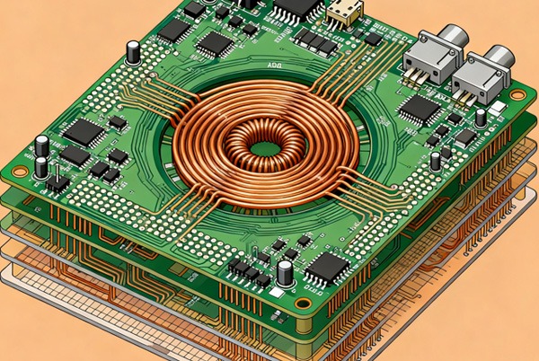
2. Stack-up and Transmission Line Design
- Symmetrical Stack-up: Structures like “Signal-Ground-Signal-Power” reduce crosstalk and impedance fluctuations.
- Microstrip vs. Stripline: Microstrip lines are cost-effective for mid-to-low frequency circuits; stripline offers better shielding for high-frequency and high-speed digital signals.
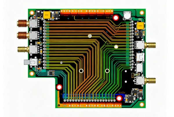
3. Impedance Matching and Via Optimization
- Control characteristic impedance (e.g., 50Ω microstrip line) by adjusting line width and dielectric thickness to minimize signal reflection.
- Use laser blind vias or via-in-pad technology to reduce parasitic effects on high-frequency signals.
4. Component Layout
- Shorten high-frequency signal paths and use zoning for digital, analog, and RF circuits to prevent interference.
Manufacturing Process Challenges & Breakthroughs
- Plated Through-Hole (PTH) Process: Address poor copper adhesion on PTFE material hole walls using plasma treatment or sodium naphthalene activation.
- Line Defect Control: Optimize etching parameters and plating processes to reduce line gaps and pitting.
- Solder Mask Adhesion: Employ acid cleaning and step-curing processes to resolve bubbling and peeling issues.
- Surface Scratch Prevention: Implement meticulous handling and equipment maintenance throughout the process to ensure surface integrity.
How to Choose a High-Frequency PCB Supplier
- Technical Capability: Assess core equipment like laser drilling and multilayer lamination, as well as custom design expertise.
- Manufacturing Experience: Prioritize suppliers with proven experience in high-volume, high-frequency PCB production to ensure process stability.
- Quality Certifications: Verify international certifications like ISO 9001 and UL to guarantee product consistency.
- Customer Reputation: Review industry case studies and user feedback to evaluate delivery capability and service levels.
Future Trends & Summary
With the proliferation of 5G, IoT, and autonomous driving technologies, high-frequency PCBs will evolve towards higher frequencies, lower loss, and greater integration. Their innovative materials and precision processes will continue to push the boundaries of electronic device performance. Selecting a technically proficient and quality-focused supplier is essential for the successful implementation of high-frequency PCBs.
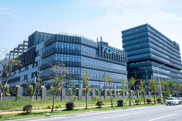
Advantages of Choosing TOPFAST
Against this backdrop of rapid technological advancement, choosing a professional supplier like TOPFAST is particularly important. TOPFAST offers comprehensive high-frequency board solutions with the following core advantages:
Technological Leadership: TOPFAST boasts a complete high-frequency board production line, including advanced laser drilling equipment, precise lamination control systems, and professional testing instruments, ensuring industry-leading product performance.
Rich Experience: Over the years, TOPFAST has accumulated extensive project experience in areas such as 5G base stations, automotive radar, and satellite communication, providing customers with full-process technical support from design to mass production.
Quality Assurance: Certified under international quality systems such as ISO9001 and IATF16949, TOPFAST has established a comprehensive quality management system to ensure product consistency and reliability.
Innovative R&D: TOPFAST operates a dedicated R&D center, continuously investing in the development of new materials and processes. Partnerships with multiple research institutions ensure the company remains at the forefront of technological innovation.
Customer Service: TOPFAST provides full-cycle customer support, from technical consultation and design assistance to after-sales service, ensuring the smooth progress and rapid implementation of customer projects.