Table of Contents
What is high speed and high frequency PCB board?
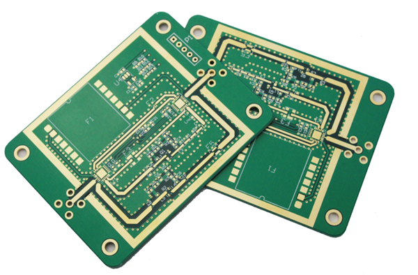
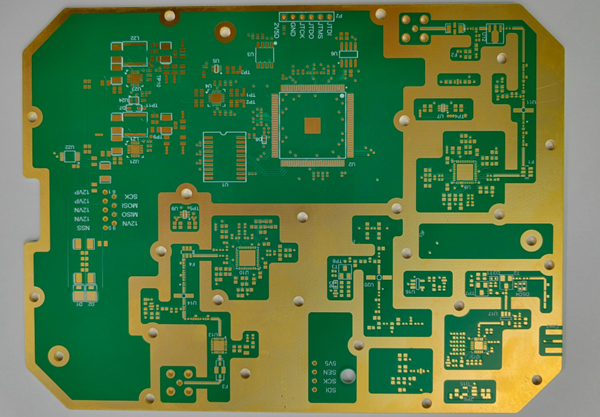
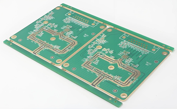
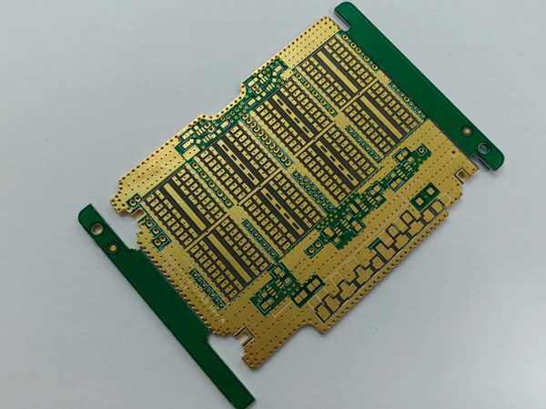
High-speed and high-frequency PCB board refers to the frequency above 1GHz printed circuit board. Its various physical properties, precision, and technical parameters require very high requirements and are commonly used in communication systems, automotive ADAS systems, satellite communication systems, radio systems, and other fields. Driven by consumer demand for faster Internet connectivity, mobile high-definition video, and the Internet of Things (IoT), high-speed, high-frequency PCBs must also support the need for high-speed digital data transmission. 5G, as well as big data centers and other commercial applications, as well as a growing number of personal applications, continue to refresh the rate of digital communications system requirements.
HF pcb design rules
- Transmission Line Theory and Matching
In high-frequency circuits, the signal line is regarded as a transmission line, and the continuity and matching of its characteristic impedance becomes critical. Improper impedance matching can lead to signal reflection, affecting signal integrity and stable system operation. Common impedance control methods include selecting the appropriate line width, line spacing, and dielectric thickness, and using specific stacking structures to achieve the desired characteristic impedance value (common as 50Ω or 75Ω). - high-frequency signal wiring skills
short and straight: high-frequency signal lines should be as short as possible and straight-line layout, reduce the corners to reduce the inductance of the signal path, and reduce transmission delay.
Layers and stacked layers: Multilayer board design helps to isolate different signals and reduce cross-talk. High-frequency signals are usually arranged in the inner layer and as close to the ground plane as possible, utilizing the ground plane as a return path to enhance the shielding effect of the signal.
Impedance control and matching: Use advanced PCB design software for simulation and analysis to ensure that the characteristic impedance of all transmission lines is the same, and implement impedance matching at the signal source and load side.
Decoupling and bypass: The purity of the power supply and ground plane in the high-frequency circuit has a great impact on the signal quality. A reasonable layout of decoupling capacitors, especially high-frequency ceramic capacitors, can effectively filter out power supply noise and maintain voltage stability.
Differential pair wiring: for high-speed differential signals, keeping the two lines of equal length and spacing, which helps to improve the signal’s anti-jamming ability, is the preferred option for high-frequency signal transmission. - electromagnetic compatibility considerations
High-frequency circuit design must strictly control EMI/EMC issues. This includes the use of appropriate shielding measures, a well-designed grounding system, reasonable arrangement of high-frequency components, and the application of filtering technology. In addition, EMC testing to ensure that the product meets the relevant electromagnetic compatibility standards is an integral part of the product development process.
Manufacturing process of HF PCB
The manufacturing process of HF PCB is relatively complex, mainly including the following steps
- Design and Layout
Firstly, according to the application requirements and signal transmission characteristics of HF PCB, circuit design and layout planning are carried out. This step needs to fully consider the signal transmission path, impedance matching, signal integrity, and other factors to ensure the performance and quality of the high-frequency PCB. - Drawing production
Transforms the circuit design and layout planning into a wiring diagram on a drawing. Drawing production needs to accurately and precisely express the layout of the circuit and the connection relationship, to subsequent manufacturing and processing. - Etching and Lamination
The circuit diagram on the drawing is transferred to the substrate by photolithography and etched to form a conductive layer. Then, the conductive layer on the film protects the line and improves mechanical strength. This step requires strict control of the etching and filming process parameters to ensure the accuracy and quality of high-frequency PCB.
Matters to be aware of in HF pcb design
In HF PCB design, signal integrity is a key indicator of system performance, preventing signal damage and errors, and safeguarding the stable operation of HF systems.
KEY DESIGN CONSIDERATIONS
Impedance control: Impedance control ensures constant trace width and spacing to adequately transmit signals and protect against impedance deviations in the signal path.
Controlled Impedance Cabling Techniques: The use of techniques such as microstrip and stripline structures helps maintain controlled impedance, minimize signal reflections, and ensure signal integrity.
Minimizing crosstalk: Carefully designed signal line spacing and shielding avoids unnecessary signal coupling and attenuates interference from poorer signals.
Grounding and Distribution: Proper distribution of power networks and reliance on large plane grounding reduces ground bounce and voltage noise to ensure signal integrity.
Through-hole location and type: Correctly place and select high-frequency through-hole structures to reduce signal distortion. Utilize high-frequency via types to mitigate signal attenuation.
Manufacturing Processes and Challenges: HF PCB manufacturing involves critical steps such as lamination, etching, and drilling, which present the following challenges:
Tighter Tolerances: HF PCBs need to maintain tight tolerances on alignment width, spacing, and dielectric constant to ensure signal integrity and impedance control.
Advanced drilling techniques: Advanced techniques such as laser drilling or controlled depth drilling are used to create through-holes, ensuring minimal signal loss and impedance variation.
Material Handling: High-frequency PCB materials are sensitive to fine handling and need to be kept under low mechanical stress and naturally friendly storage conditions.
High-frequency signal pcb alignment
First of all, the design of high-frequency circuits requires special attention to the transmission characteristics of the signal. In multilayer PCB boards, a reasonable choice of layers and dimensions can make full use of the intermediate layer for shielding, to realize the proximity of grounding, reduce parasitic inductance, shorten the signal transmission path, reduce the signal cross-interference, and improve the reliability of the circuit.
However, with the increase in the number of PCB layers, the manufacturing process becomes more complex and the cost rises. Therefore, in addition to choosing the right number of PCB layers, reasonable component layout and wiring planning are also required during design. The following is a summary of some of the experience of high-frequency wiring:
- Reduce lead layer alternation: In the process of component connection, minimize the use of vias, because each vias will bring additional distributed capacitance, affecting the speed and stability of signal transmission.
- shorten the lead length: the radiation intensity of high-frequency signals is directly proportional to the length of the alignment, therefore, for high-frequency signal lines such as clocks, crystals, etc., the length of the alignment should be shortened as much as possible to reduce coupling interference.
- Avoid lead bending: in high-frequency circuit wiring, should try to use straight lines, such as the need to turn, should be used 45-degree folding line or arc, to reduce the signal to the outside of the emission and coupling.
- control crosstalk: crosstalk is the signal line due to electromagnetic field coupling between the undesired noise. To reduce crosstalk, crosstalk can be serious lines between the insertion of ground or ground plane, increase the spacing of signal lines, or in adjacent layers using vertical alignment.
- Isolation of digital and analog ground: high-frequency digital signal ground and analog signal ground should be isolated to prevent high-frequency harmonics from interfering with analog signals through ground coupling.
- Increase the decoupling capacitance: Increase the high-frequency decoupling capacitance near the power supply pins of the IC block, which can suppress the high-frequency harmonics on the power supply pins and reduce the interference.
- Avoid the formation of loops: high-frequency signal alignment should avoid the formation of loops, if unavoidable, should minimize the loop area.
- Ensure signal impedance matching: impedance mismatch will lead to signal reflection, affecting signal stability. Therefore, the characteristic impedance of the signal transmission line should be equal to the load impedance, to avoid sudden changes or corners of the transmission line.
When designing high-speed PCB wiring, it is also necessary to comply with specific wiring rules, such as the differential alignment rules for signals such as LVDS, USB, HDMI, and DDR, in order to control the impedance of signal pairs and reduce crosstalk.
PCB wiring to reduce high-frequency signal crosstalk
In high-frequency circuit design, crosstalk between signal lines is a problem that requires special attention. Crosstalk refers to the coupling phenomenon between the signal lines are not directly connected, it will have a serious impact on the performance and reliability of the circuit. The following are some effective measures to reduce crosstalk of high-frequency signals
Inserting a ground or ground plane: Inserting a ground or ground plane between two lines with serious crosstalk can serve as an isolation, thus reducing crosstalk.
Arrangement of large area ground: If it is impossible to avoid parallel distribution, you can arrange a large area of “ground” on the opposite side of the parallel signal lines to significantly reduce the interference.
Increase the spacing of signal lines: Under the premise of wiring space permits, increasing the spacing between adjacent signal lines can reduce the parallel length of signal lines, thus reducing crosstalk.
Vertical alignment: If the parallel alignment within the same layer can not be avoided, in the two adjacent layers, the direction of the alignment is perpendicular to each other, which can effectively reduce crosstalk.
Surrounding the clock line: the clock line should be surrounded by ground wires, and more ground holes to reduce the distribution capacitance, thereby reducing crosstalk.
The use of low-voltage differential clock signal: the high-frequency signal clock as much as possible to use low-voltage differential clock signal and packet ground, which can effectively reduce crosstalk.
Ground or connect to the power supply: idle inputs do not hang, but will be connected to the ground or connected to the power supply, which can reduce unnecessary interference.
HF PCB Application Scope
HF PCB plays an important role in many fields due to its excellent performance and wide range of application scenarios. The following are some of the major application areas:
- Communication Equipment
High-frequency PCBs play a vital role in communication equipment. They are widely used in equipment such as telephones, cellular phones, radios, satellite communication systems, etc., to provide reliable signal transmission paths and ensure accurate data transmission. The excellent performance of high-frequency PCBs enables communication equipment to maintain stable communication quality in complex and changing environments. - Medical Equipment
Medical equipment has extremely high requirements for precision and reliability. High-frequency PCBs are widely used in medical diagnostic and monitoring equipment, surgical instruments, implantable devices, and so on because of their high precision and stability. HF PCB can ensure the normal operation of medical equipment and patient safety. - Industrial Control Systems
High-frequency PCBs play a key role in industrial control systems. They are used in a variety of automation equipment, such as robots, CNC machine tools, production line automation, etc., to achieve precise control and operation. The excellent performance of HF PCBs enables industrial control systems to operate efficiently and stably. - Automotive Electronics
A large number of high-frequency PCBs are used in automobiles, including engine control modules, body control modules, airbag control systems, and so on. These circuit boards control the vehicle’s various systems and ensure their normal operation. The excellent performance of high-frequency PCBs enables automotive electronic systems to maintain stable performance in complex and changing driving environments. - Aerospace
The aerospace field requires a high degree of reliability and precision in equipment. High-frequency PCB because of its excellent performance and stability, is widely used in aircraft, rockets, satellites, etc., in order to achieve a variety of complex control and monitoring functions. The excellent performance of high-frequency PCBs enables aerospace equipment to maintain stable operation in extreme environments. - Computers and Servers
Computers and servers also require the use of a large number of high-frequency PCBs. These boards provide reliable signal transmission paths and ensure fast data transmission and processing. The excellent performance of high-frequency PCBs enables computers and servers to operate at high speeds while maintaining stable performance. - Internet of Things (IoT)
The number of IoT devices is huge and needs to realize various intelligent functions. High-frequency PCBs provide stable and reliable control and data transmission paths for IoT devices, thus realizing intelligent management and remote monitoring of the devices. The wide application of high-frequency PCBs promotes the rapid development of IoT technology.
In short, the design of high-frequency circuits is a complex process that requires comprehensive consideration of signal transmission, electromagnetic interference, cost and manufacturing process, and other factors. Through a reasonable choice of PCB layers, and careful planning of component layout and wiring, we can design both efficient and reliable high-frequency circuits to meet the needs of modern electronic equipment for high performance.