Technologie de montage en surface
High-Precision
Assemblage SMT
Services
Zero-defect PCBA solutions · 24h turnaround · Sub-micron accuracy · Full supply chain
0
Years Experience
0
Global Clients
0
Prototype Turnaround
0
AOI Inspection Rate
What We Do
Précision
Fabrication
Excellence
End-to-end PCBA solutions built on industrial grade equipment and a zero-defect commitment. From bare board to finished product, one trusted partner.
Demande de devis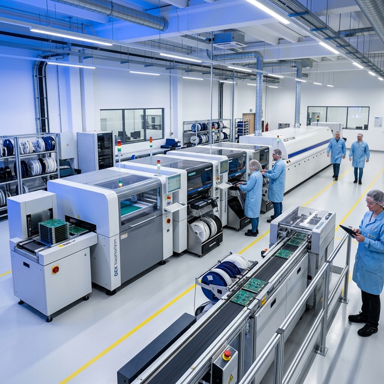
01
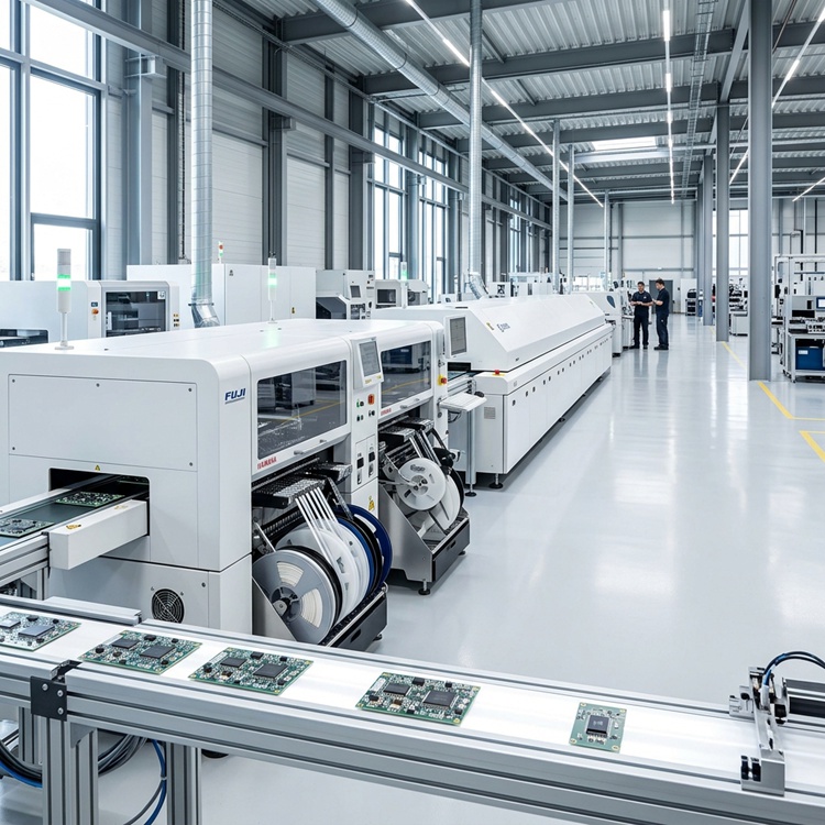
Advanced SMT Assembly
01005 & fine-pitch BGA placement at ±0.03mm accuracy with Yamaha high-speed lines.
01005 Min.
±0.03mm
120K CPH
02
THT / Mixed Assembly
Heavy-duty through-hole soldering for power electronics and industrial controls.
Mixed PCB
Wave + Selective
03
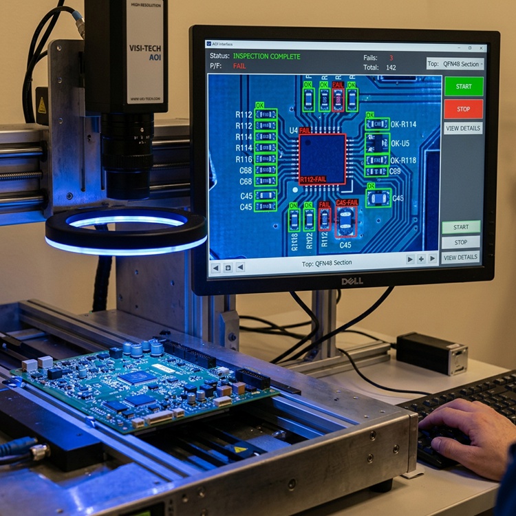
3D AOI & X-Ray Inspection
100% automated coverage meeting IPC-A-610 Class 3. Every board cleared before shipment. Zero tolerance for defects.
AOI 3D
X-Ray AXI
IPC Class 3
04
Full Turnkey Supply Chain
Global component sourcing, PCB fabrication, PCBA, functional testing, and logistics — one partner, total visibility.
Global Sourcing
Clé en main
05
Prototype to Mass Production
Engineering prototypes in 24 hours scaling seamlessly to 1M+ units per month with no change in quality standards.
24h Proto
1M+ units/mo
How We Build
Fabrication
Workflow
Every board follows a battle-tested four-stage flow engineered for defect-free output.
01
Pâte à braser
Pâte à braser
Printing
Automated stencil printing with 3D SPI at every board — micron-level paste validation.
02
Pick & Place
Pick & Place
Mounting
High-speed Yamaha / Panasonic lines placing 01005 passives at ±0.03mm repeatability.
03
Nitrogen
Nitrogen
Reflow Oven
Multi-zone nitrogen reflow with precision thermal profiling for every board type.
04
3D AOI &
3D AOI &
X-Ray Audit
100% inline automated optical and X-ray inspection. Zero tolerance for defects.
Paramètres techniques
Detailed
Spécifications
Every parameter engineered to meet the most demanding standards in electronics manufacturing.
01005Min. Component
±0.03mmPrécision du placement
32LMax. Layer Count
Min. Component01005 (0.4 × 0.2mm)
Précision du placement±0.03mm
BGA Fine Pitch0.35mm
Max. Component Height25mm
Line Throughput120,000 CPH
MatériauxFR4, Aluminum, Rogers, Flex
Max. Board Size500 × 450mm
Épaisseur du panneau0.4 – 4.0mm
Layer Capability1 – 32 Layers
Min. Lead Time24 Hours (Prototype)
Paste Inspection3D SPI
Post-ReflowAOI 3D
BGA Joints3D X-Ray (AXI)
Test fonctionnelTIC / FCT
StandardIPC-A-610 Classe 3
Common Questions
FAQ
We require Gerber files (RS-274X), a BOM (Bill of Materials) in Excel format, and a CPL (Centroid / Pick & Place file).
Yes. We specialise in high-density components. Our 3D X-Ray inspection ensures all BGA solder joints are void-free.
We offer full turnkey (we source all components), partial turnkey, or fully consigned (you provide components) assembly. All options include free DFM review.
No MOQ. We support single prototype boards through to millions of units in mass production, with the same quality standards applied at every volume.
Start Your Project
Get a Free
Engineering Quote
Our engineers review every submission within 8 business hours. Upload your design files and we'll handle the rest.
- No minimum order quantity
- Engineering prototype in 24h
- IPC-A-610 Class 3 quality
- Free DFM analysis included
- Dedicated account engineer
ISO 9001IPC CLASS
3ROHSUL
Contactez nous
Parlez à notre expert en PCB