Die Elektronikindustrie wächst schnell. Das bedeutet, dass gedruckte Schaltplatten (PCBs), die wichtigsten Komponenten elektronischer Geräte, müssen kontinuierlich verbessert werden. Dieser Artikel befasst sich mit den Schlüsseltechnologien für die Fehlererkennung bei PCBs. Dazu gehören optische Inspektionstechnologie, elektrische Prüftechnologie, Wärmebildtechnologie, Röntgeninspektion und akustische Prüfverfahren.
Es untersucht die verschiedenen Technologien und ihre Funktionen sowie die Vor- und Nachteile der einzelnen Technologien. Außerdem wird untersucht, wie maschinelles Lernen und künstliche Intelligenz zur Fehlererkennung eingesetzt werden können. Durch den Vergleich verschiedener Situationen und anhand realer Beispiele werden die Konzepte erläutert und technische Informationen bereitgestellt, die zur Qualitätskontrolle bei der Leiterplattenherstellung beitragen.
Inhaltsübersicht
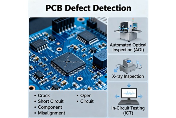
Arten von PCB-Defekten und ihre Auswirkungen
Häufige Fehler im Leiterplattenherstellungsprozess sind:
- Kurzschlüsse und Unterbrechungen: Abnormale Verbindungen oder Unterbrechungen zwischen Leitern.
- Lötstellenfehler: Kalte Lötstellen, Lötperlen usw.
- Substratschaden: Delaminierung, Risse, Verformung.
- Qualitätsprobleme bei Lochwänden: Ungleichmäßige Verkupferung, Rückstände in Bohrungen.
- Fehlausrichtung oder Fehlen von Komponenten: Montagefehler.
Diese Defekte können zu Funktionsausfällen der Schaltkreise, verminderter Zuverlässigkeit oder sogar zu Schäden am Gerät führen, weshalb effiziente und genaue Erkennungstechnologien von entscheidender Bedeutung sind.
Forschung zu Schlüsseltechnologien
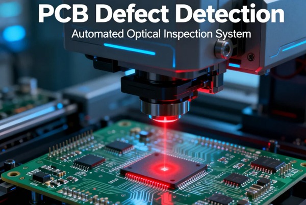
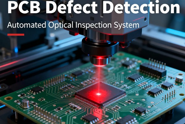
1. Optische Inspektionstechnologie
Bei der optischen Inspektion werden mit hochauflösenden Kameras Bilder der Leiterplattenoberfläche aufgenommen und Bildverarbeitungsalgorithmen kombiniert, um Fehler zu identifizieren. Zu den wichtigsten Methoden gehören:
- Automatisierte optische Inspektion (AOI): Nutzt Mehrwinkelbeleuchtung und Farbfilterung, um den Kontrast von Fehlern zu verbessern und die Form von Lötstellen, die Platzierung von Bauteilen usw. zu erkennen.
- 3D-Scan-PrüfungErfasst 3D-Topografiedaten durch Laserscanning oder strukturierte Lichtprojektion, um höhenbezogene Fehler (z. B. Verformungen, Lötpastendicke) zu erkennen.
Vorteile: Berührungslos, schnell, geeignet für großflächige Inspektionen.
BeschränkungenEmpfindlich gegenüber Oberflächenreflexionen oder transparenten Materialien, eingeschränkte Fähigkeit zur Erkennung innerer Fehler.
2. Elektrische Prüftechnik
Bei elektrischen Prüfungen werden Fehler durch Messung der elektrischen Parameter von Schaltkreisen beurteilt:
- Flying Probe TestVerwendet bewegliche Sonden zur Messung von Widerstand, Kapazität und Spannung zwischen Knotenpunkten.
- Nagelbett-Test: Kontaktiert gleichzeitig mehrere Testpunkte über kundenspezifische Vorrichtungen, geeignet für die Massenproduktion.
Vorteile: Überprüft direkt die elektrische Leistung, hohe Genauigkeit bei der Erkennung von Unterbrechungen/Kurzschlüssen.
BeschränkungenErfordert physischen Kontakt, hohe Kosten für Testvorrichtungen, nicht in der Lage, nicht-elektrische Defekte zu lokalisieren.
3. Wärmebildtechnologie
Verwendet Infrarot-Wärmebildkameras, um die Temperaturverteilung von Leiterplatten während des Betriebs zu erfassen und Defekte (z. B. Überhitzung aufgrund von Kurzschlüssen) durch ungewöhnliche Temperaturanstiege zu lokalisieren.
Vorteile: Berührungslose Echtzeitüberwachung dynamischer Fehler.
Beschränkungen: Wird von der Umgebungstemperatur beeinflusst, erfordert thermische Modelle für die Analyse.
4. Röntgeninspektionstechnologie
Röntgenstrahlen durchdringen die innere Struktur von Leiterplatten und erzeugen 2D- oder 3D-Bilder, die zur Erkennung folgender Fehler verwendet werden:
- Innere Hohlräume in Lötstellen, BGA-Lötkugelverbindungenundgnale Pfade mit CAD-Software verdeckte Verkabelung.
Vorteile: Kann interne und Verpackungsfehler erkennen.
BeschränkungenHohe Ausrüstungskosten, erfordert Strahlenschutz und komplexe Analysen.
5. Akustische Mikrobildgebung
Scans die innere Struktur von Leiterplatten mit Ultraschall und erkennt Defekte wie Delamination und Risse anhand von akustischen Wellenreflexionssignalen.
Vorteile: Empfindlich gegenüber internen Materialstrukturen.
BeschränkungenErfordert ein Kopplungsmedium, relativ geringe Auflösung.
Technologievergleich und Anwendungsauswahl
Die folgende Tabelle vergleicht die Eigenschaften der wichtigsten Erkennungstechnologien:
| Technologietyp | Erkennungsziel | Präzision | Geschwindigkeit | Kosten | Anwendbare Szenarien |
|---|---|---|---|---|---|
| Optische Inspektion (AOI) | Oberflächenfehler | Hoch | Schnell | Mittel | Lötstellen, Bauteilplatzierung |
| Elektrische Prüfung | Elektrische Leistung | Sehr hoch | Mittel | Mittel-Hoch | Shorts/Offen |
| Wärmebildgebung | Thermische Anomalien | Mittel | Schnell | Mittel | Überhitzungsfehler |
| Röntgenbild | Interne Struktur | Hoch | Langsam | Hoch | BGA, Lochfehler |
| Akustische Mikrobildgebung | Interne Delaminierung | Mittel-Hoch | Langsam | Hoch | Materialfehler des Substrats |
In der Praxis sollten kombinierte Strategien auf der Grundlage von Fehlertypen, Produktionsumfang und Kostenbudget ausgewählt werden. Zum Beispiel:
- Hochdichte Platten: AOI + Röntgen.
- Massenproduktion: AOI + Elektrische Prüfung.
- Überprüfung der Verlässlichkeit: Wärmebildgebung + Akustikprüfung.
Zukünftige Forschungsrichtungen
- Multimodale FusionserkennungKombination von optischen, Röntgen- und elektrischen Daten zur Verbesserung der Erkennungsabdeckung.
- Künstliche Intelligenz und maschinelles Lernen: Training von Deep-Learning-Modellen zur automatischen Erkennung von Fehlern und Reduzierung von Fehlalarmen.
- Echtzeit-Online-Erkennungssysteme: In Produktionslinien integriert für sofortiges Feedback und Prozessanpassungen.
- Miniaturisierung und hochauflösende SensorenVerbesserung der Fähigkeit, Mikrofehler (z. B. Lötstellen von 01005-Bauteilen) zu erkennen.
Schlussfolgerung
Die Technologie zur Erkennung von Leiterplattenfehlern ist ein zentraler Faktor für die Qualitätssicherung elektronischer Produkte. Verschiedene Erkennungsmethoden haben ihre eigenen Vorteile und sollten flexibel entsprechend den tatsächlichen Anforderungen ausgewählt werden. Mit der Weiterentwicklung der künstlichen Intelligenz und der Sensortechnologien werden sich die Erkennungsgenauigkeit, Effizienz und Automatisierungsgrade in Zukunft weiter verbessern und zuverlässigere Lösungen für die Qualitätskontrolle bieten. PCB-Herstellung Industrie.