Inhaltsübersicht
1. Einführung in Leiterplatten und Kernkomponenten
Gedruckte Schaltungen (PCBs) sind grundlegende Komponenten in der Elektronikindustrie. Zu ihren Hauptfunktionen gehören Signalübertragung, physische Unterstützung, Stromverteilungundgnale Pfade mit CAD-Software WärmemanagementEine Leiterplatte besteht aus verschiedenen speziellen Elementen: dem Siebdruck-Schicht (Overlay) zur Identifizierung von Komponenten, Oberflächenbeschaffenheiten (wie ENIG, HASL), Leiterbahnen für elektrische Verbindungen zwischen den Schichten, Durchsteckbauteile (PTH) und Oberflächenmontierte Bauelemente (SMD), Kupfer gießt (Polygon), Wärmeleitpads, Signalverläufe (Spur) und Polster, neben anderen wichtigen Funktionen.
2. PCB-Klassifizierungssystem
2.1 Klassifizierung nach Substratmaterial
Keramische Substrate: Utilizing materials like Alumina (Al₂O₃), Aluminum Nitride (AlN), or Silicon Carbide (SiC), these offer exceptional thermal conductivity and are designed for high-temperature environments and high-power applications.
Metallkern-Leiterplatten (MCPCBs): Dazu gehören Substrate auf Aluminium- und Kupferbasis, die für ihre hervorragende Wärmeableitung bekannt sind und häufig in Hochleistungsschaltungen und LED-Beleuchtungen verwendet werden.
Papierbasierte Substrate: Wie beispielsweise die Typen FR-1 und FR-2, verwenden Faserverstärkungen, sind mit Harz imprägniert und mit Kupferfolie laminiert und eignen sich in erster Linie für ein- oder doppelseitige Leiterplatten.
Verbundsubstrate: Kombinieren Sie auf innovative Weise die Eigenschaften mehrerer Materialien, z. B. CEM-2 (Epoxidharz mit Papierkern und Glasgewebeoberflächen), um spezifische Leistungsanforderungen zu erfüllen.
2.2 Klassifizierung nach strukturellen Merkmalen
Starre PCBsVerwenden Sie nicht biegsame, starre Substrate, darunter verschiedene Typen wie FR-4 (Glas-Epoxid), papierbasierte, Verbund-, Keramik- und Metallkernplatten.
Flexible PCBs (Flex-Leiterplatten): Verwenden flexible isolierende Substrate, die sich biegen, rollen und falten lassen und somit ideal für die beengten Platzverhältnisse in tragbaren elektronischen Geräten sind.
Starrflexible Leiterplatten: Integrieren Sie starre und flexible Zonen auf intelligente Weise und bieten Sie sowohl strukturelle Festigkeit als auch Flexibilität bei der Installation.
HDI-Platinen (High-Density Interconnect): Nutzt Microvia-Technologie und ultradünne Kupferfolien, um den Anforderungen an die Miniaturisierung elektronischer Geräte gerecht zu werden. Zu den Strukturen gehören 2-stufige gestapelte Durchkontaktierungen, 2-stufige versetzte Durchkontaktierungen und 1-stufige HDI.
IC-Substrate: Speziell für die Chipverpackung entwickelt, bietet wichtige Funktionen wie elektrische Verbindung, physischen Schutz, strukturelle Unterstützung und Wärmemanagement.
3. Eingehende Analyse der PCB-Substrattechnologie
3.1 Schichtaufbau
Moderne Leiterplatten zeichnen sich durch ein mehrschichtiges Design aus:
- KernLaminat aus Glasfasergewebe und Epoxidharz, beidseitig mit Kupfer beschichtet.
- Prepreg (Vorimprägniert): Ein Verbundwerkstoff aus Glasfasergewebe und teilweise ausgehärtetem Harz, der beim Laminieren für die Verbindung der Schichten sorgt.
- Kupfer-Folie: Divided into Electro-Deposited (ED) copper (preferred for rigid boards) and Rolled Annealed (RA) copper (used for flexible boards). Thickness is measured in ounces (OZ), e.g., 1 OZ (≈35µm).
3.2 Via Technologies
PCB-Verbindungsdurchkontaktierungen werden in drei Typen unterteilt:
- Durchkontaktierung: Durchläuft alle Schaltungsschichten.
- Blind ViaVerbindet eine äußere Schicht mit einer oder mehreren inneren Schichten, durchdringt jedoch nicht die gesamte Platine.
- Begraben über: Befindet sich vollständig innerhalb der inneren Schichten und verbindet zwei oder mehr innere Schichten, ohne die Außenflächen zu erreichen.
3.3 Wichtige Leistungsparameter
Thermische Parameter:
- Tg (Glasübergangstemperatur): Der kritische Punkt, an dem das Harz von einem starren in einen weicheren Zustand übergeht, was sich direkt auf die Wärmebeständigkeit des Substrats auswirkt.
- Td (Zersetzungstemperatur): Die Temperatur, bei der das Harz aufgrund thermischer Zersetzung 5 % seiner Masse verliert.
- CTE (Coefficient of Thermal Expansion): Determines dimensional stability under temperature variations. Typically X/Y: 16-18 ppm/°C, Z: 40-60 ppm/°C.
Elektrische Parameter:
- Dk (Dielectric Constant): Influences signal propagation speed and characteristic impedance. A lower Dk generally allows faster signal speed (V = C/√Dk).
- Df (Verlustfaktor): Beeinflusst die Signalintegrität und -qualität; ein niedrigerer Df-Wert bedeutet weniger Signalverlust.
- Oberflächen-/Volumenwiderstand: Misst die Leitfähigkeit.
Mechanische Parameter:
- Biegefestigkeit und Schälfestigkeit
- Wasseraufnahme: Beeinflusst die Stabilität und Zuverlässigkeit des Untergrunds. Feuchtigkeit kann den Dk-Wert erhöhen und das Risiko einer Delaminierung („Popcorning“) erhöhen.
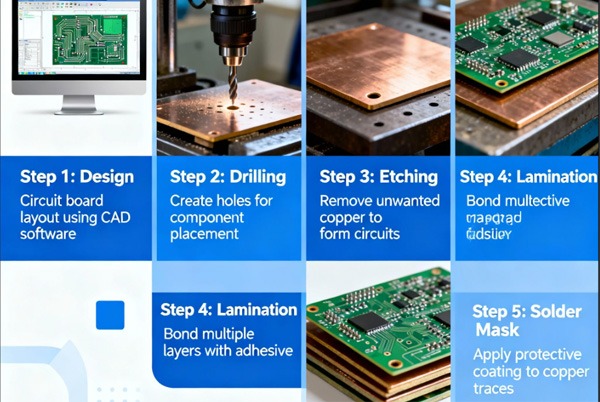
4. Präzisions-Leiterplattenfertigungsprozessablauf
Die Leiterplattenherstellung folgt einer strengen Abfolge:
- Inner Layer Imaging → 2. Fotolack-Laminierung → 3. Exposition → 4. Entwicklung → 5. Ätzen → 6. Streifenresist → 7. Schichtstapelung → 8. Kaschierung → 9. Bohren → 10. Plattierung (PTH) → 11. Außenlage Resist-Laminierung → 12. Exposition → 13. Entwicklung → 14. Musterbeschichtung (Cu/Sn) → 15. Streifenresist → 16. Ätzen → 17. Blechstreifen → 18. Siebdruck/Beschriftungsdruck → 19. Oberfläche
5. Umfassender Vergleich von Oberflächenbehandlungen
| Oberfläche | Wichtigste Merkmale und Vorteile | Einschränkungen / Herausforderungen | Kostenniveau | Thickness Range (µm) | Haltbarkeitsdauer |
|---|---|---|---|---|---|
| HASL (bleifrei) | Geeignet für große Polster, großer Abstand | Nicht ideal für HDI; hohe Temperatur; unebene Oberfläche | Mittel-Hoch | 2-5 (auf dem Pad) | 12 Monate |
| HASL (bleihaltig) | Hervorragende mechanische Festigkeit | Umweltbelange (Pb-Gehalt) | Mittel-Hoch | 2-5 (auf dem Pad) | 12 Monate |
| OSP | Einfacher Prozess, geringe Kosten | Nicht für mehrfache Reflows geeignet; schwierige Inspektion | Niedrigste | 0.1 – 0.5 | 6 Monate |
| ENIG (Chemisch Nickel/Immersionsgold) | Zuverlässiges Löten, ebene Oberfläche, gute Korrosionsbeständigkeit | Potenzial für „Black Pad“ (Ni-Korrosion), „Gold Embrittlement“ | Hoch | Ni: 3-5 / Au: 0,03-0,08 | 12 Monate |
| ENEPIG (Chemisch Nickel/Palladium/Immersionsgold) | Hochwertige Anwendungen, hervorragende Korrosionsbeständigkeit, drahtbondfähig | Komplexe Prozesssteuerung, Potenzial für schwarze Flecken/Verfärbungen | Hoch | Ni: 2–5 / Pd: 0,05–0,15 / Au: 0,05–0,15 | 6 Monate |
| Immersionssilber (ImAg) | Flache Oberfläche, geeignet für mehrere Reflow-Prozesse | Verfärbt sich leicht, erfordert strenge Lagerbedingungen | Mittel | 0.1 – 0.5 | 12 Monate |
| Tauchzinn (ImSn) | Gute Ebenheit, Lötbarkeit | Risiko von Zinnwhiskern, schlechte Wärmealterungsbeständigkeit | Low | 0.8 – 1.2 | 6 Monate |
| Elektrolytisches Ni/Au (Weiches Gold) | Hervorragende Verschleißfestigkeit, Kontaktzuverlässigkeit | Hoher Goldverbrauch, mögliche Probleme mit der Haftung der Lötmaske auf Gold | Höchste | Ni: 3-5 / Au: ≥0.05 (selective) | 12 Monate |
| Elektrolytisches Hartgold | Extreme Verschleißfestigkeit (z. B. für Finger) | Höchste Kosten, komplexester Prozess | Höchste | 0,3 – 3,0 (bei Kontakt) | 12 Monate |