
Gedruckte Schaltungen (PCBs) sind die Grundpfeiler moderner elektronischer Geräte. Da Geräte immer höhere Frequenzen, höhere Geschwindigkeiten und eine immer stärkere Miniaturisierung aufweisen, ist ein ausgezeichnetes PCB-Layout-Design zu einem entscheidenden Faktor für die Produktleistung geworden. Dieser Artikel befasst sich mit fortschrittlichen PCB-Layout-Techniken wie Hochgeschwindigkeits-Routing, Impedanzkontrolle und Optimierung der Stromintegrität, die Ingenieuren dabei helfen, zuverlässigere und effizientere Leiterplatten zu entwerfen.
Inhaltsübersicht
Hochgeschwindigkeits-Routing-Technologie
Prinzip der kurzen und geraden Spur
Die Hochgeschwindigkeits-Signalführung sollte dem Prinzip des SchuhsOptimieren Sie den Leiterbahnverlauf und minimieren Sie unnötige Biegungen und Kurven. Durch die Beibehaltung einer konsistenten Leiterbahngeometrie wird das Risiko von Signalverzögerungen und -verzerrungen erheblich reduziert.
Wichtige Punkte zur Umsetzung:
- Priorisieren Sie die Verlegung kritischer Hochgeschwindigkeits-Signalwege.
- Vermeiden Sie 90-Grad-Winkel; verwenden Sie stattdessen 45-Grad-Winkel oder Bogenkurven.
- Halten Sie eine einheitliche Leiterbahnbreite und einen einheitlichen Abstand ein.
Differentialpaar-Routing-Strategie
Differential Signal Routing ist eine effektive Methode zur Bekämpfung von Elektromagnetische Störung (EMI) und Übersprechen:
| Vorteil | Implementierungsmethode |
|---|---|
| Starke Gleichtakt-Störunterdrückung | Strenge Längenanpassung für Differentialpaare einhalten. |
| Reduzierte EMI-Strahlung | Kontrollieren Sie den gleichmäßigen Abstand innerhalb des Differentialpaares. |
| Verbesserte Signalintegrität | Vermeiden Sie Spaltungen in Referenzebenen unter Differentialpaaren. |
Optimierung der Komponentenanordnung
Durch strategische Platzierung der Komponenten lässt sich die Signalleitungsfläche erheblich reduzieren:
- Partitionslayout nach Funktionsmodulen.
- Verkürzen Sie die Verbindungswege zwischen Hochgeschwindigkeitsgeräten.
- Vermeiden Sie die Nähe zwischen empfindlichen Signalleitungen und Störquellen.
Impedanzregelungstechnologie
Beziehung zwischen Leiterbahnbreite und Impedanz
Erreichen Sie die gewünschte charakteristische Impedanz durch präzise Berechnung und Anpassung der Leiterbahnbreite:
Gängige Strategien zur Impedanzsteuerung:
- Use Impedanzberechnungstools für eine genaue Simulation.
- Berücksichtigen Sie die PCB-Lagenaufbau-Struktur und die Eigenschaften des dielektrischen Materials.
- Legen Sie entsprechende Impedanzziele für verschiedene Signaltypen fest.
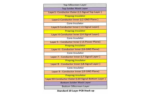
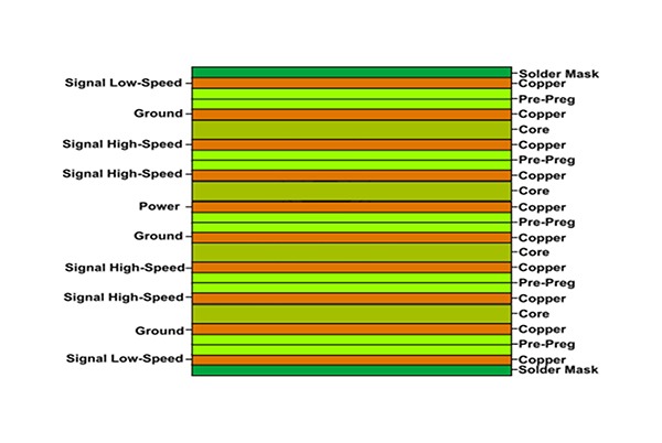
Optimierung des Stapelaufbaus
Ein rationales Stapeldesign gewährleistet eine gleichmäßige Impedanz über die gesamte Platine hinweg:
Empfohlen 4-lagiger Stapelaufbau Struktur:
Oberste Schicht: Signalschicht (Mikrostreifenstruktur)
Schicht 2: Massefläche
Schicht 3: Stromfläche
Unterste Schicht: Signalschicht (Streifenleitungsstruktur)
Auswahl des dielektrischen Materials
Auswählen stabile dielektrische Materialien ist entscheidend für die Impedanzsteuerung:
- Achten Sie auf die Dielektrizitätskonstante (Dk) und den Verlustfaktor (Df) des Materials.
- Berücksichtigen Sie Temperaturstabilität und Frequenzcharakteristik.
- Priorisieren Sie verlustarme Materialien für Hochfrequenzanwendungen.
Optimierung der Stromintegrität
Entkopplungskondensator-Layoutstrategie
Entkopplungskondensatoren sind die erste Verteidigungslinie zur Aufrechterhaltung der Stromstabilität:
Stufenweises Entkopplungsschema:
- Bulk Capacitors (10-100μF): An den Stromanschlüssen angebracht, um niederfrequente Schwankungen auszugleichen.
- Medium Capacitors (0.1-1μF): Über den gesamten Bereich verteilt, um den mittleren Frequenzbereich abzudecken.
- Small Capacitors (0.01-0.1μF): In der Nähe der Stromanschlüsse des Geräts platziert, um hochfrequente Störgeräusche zu unterdrücken.
Niederohmiges Stromverteilungsnetz (PDN)
Methoden zum Aufbau eines PDN mit niedriger Impedanz:
- Verwenden Sie massive Strom- und Masseflächen.
- Verwenden Sie Durchkontaktierungen sinnvoll, um die Stromversorgung zwischen verschiedenen Schichten herzustellen.
- Reduzieren Sie die Serieninduktivität im Strompfad.
Power Integrity Simulation
Verwenden Sie Tools wie SPICE and HyperLynx für die Simulation im Frühstadium:
- Identifizieren Sie potenzielle Probleme mit Stromrauschen.
- Optimieren Sie die Anzahl und Platzierung der Entkopplungskondensatoren.
- Überprüfen Sie den Spannungsabfall und die Rauschmarge.
Methoden zur Minderung von EMI/EMV
Optimierung der Erdungstechnik
Eine ordnungsgemäße Erdung ist die Grundlage für das EMV-Design:
Wichtige Punkte beim Erdungsdesign:
- Verwenden Sie durchgehende, massive Masseflächen.
- Stellen Sie den kürzesten Rückweg für Hochfrequenzsignale bereit.
- Vermeiden Sie Spalten und Lücken in der Grundplatte.
Abschirmungs- und Filtertechniken
Verwenden Sie eine Kombination verschiedener Methoden, um EMI zu unterdrücken:
| Techniktyp | Anwendungsszenario | Implementierungsmethode |
|---|---|---|
| Abschirmung | Schutz empfindlicher Schaltkreise | Metallabschirmungen, leitfähige Beschichtungen |
| Filtern | Unterdrückung von leitungsgebundenen Störungen | EMI-Filter, Ferritperlen |
| Kündigung | Reflexionen reduzieren | Quellen-/Endanpassungswiderstände |
Strategien zum Wärmemanagement
Kühlkörperdesign und -layout
- Wählen Sie entsprechend der Verlustleistung Kühlkörper in geeigneter Größe aus.
- Stellen Sie einen guten Kontakt zwischen dem Kühlkörper und der Chipoberfläche sicher.
- Erwägen Sie, die Ausrichtung des Kühlkörpers an der Luftströmungsrichtung auszurichten.
Thermische Durchkontaktierungen und Wärmeleitpads
- Anordnung von thermischen Durchkontaktierungen unter wärmeerzeugenden Bauteilen.
- Use thermal pads to increase the散热 area.
- Leitet Wärme effektiv zu internen Masseflächen.
Luftstrommanagement
- Berücksichtigen Sie bei der Platzierung der Komponenten die Luftströmungswege.
- Platzieren Sie Komponenten, die hoher Hitze ausgesetzt sind, stromaufwärts im Luftstrom.
- Vermeiden Sie hohe Komponenten, die den Luftstrom behindern.
Grundsätze der Fertigungsgerechtigkeit (DFM)
Wichtige Punkte zum DFM
Die Umsetzung von DFM-Prinzipien kann die Produktionseffizienz und den Ertrag erheblich verbessern:
Kritische DFM-Prüfpunkte:
- Die Mindestspurbreite/-abstand entspricht den Möglichkeiten des Herstellers.
- Optimierte Bohrlochgrößen und -positionen.
- Standardisiertes Design für Lötmaske und Siebdruck.
- Berücksichtigung der Plattenkante und des Panelisierungsdesigns.
Einsatz fortschrittlicher DFM-Tools
- Verwenden Sie Tools wie PCBCart Sofortige DFM für die Vorabprüfung des Entwurfs.
- Erhalten Sie Echtzeit-Feedback zur Herstellbarkeit.
- Identifizieren und beheben Sie potenzielle Probleme frühzeitig.
Besondere Überlegungen zum Layout von Mixed-Signal-Leiterplatten
Analoge und digitale Partitionierung
Behandeln Sie die Beziehung zwischen analogen und digitalen Schaltungen korrekt:
Grundsätze für die Aufteilung des Layouts:
- Analoge und digitale Schaltungsbereiche physisch trennen.
- Verwenden Sie unabhängige Strom- und Masseflächen.
- Führen Sie eine Einpunkt-Erdung an ADC/DAC-Geräten durch.
Mixed-Signal-Erdungsstrategien
Wählen Sie das geeignete Erdungsschema basierend auf der Komplexität des Systems:
Einzelnes Masseflächenschema (Geeignet für Systeme mit niedrigem Digitalstrom):
- Verwenden Sie eine einzige, durchgehende Massefläche.
- Lassen Sie analoge und digitale Rückströme auf natürliche Weise trennen.
Geteilte Grundplatte (Geeignet für Systeme mit hohem Digitalstrom):
- Analoge und digitale Erdungen trennen.
- Anschluss an einem einzigen Punkt in der Nähe der Stromversorgung (Sternpunkt).
- Sorgen Sie für klare Erdungspfade für Mixed-Signal-Geräte.
PCB-Layout-Checkliste
Verwenden Sie die folgende Checkliste für die abschließende Überprüfung nach Fertigstellung des Layouts:
- Signalintegritätsprüfung (Hochgeschwindigkeits-Signalwege, Terminierung, Impedanz)
- Überprüfung der Stromintegrität (Entkopplung, PDN-Impedanz)
- Bewertung des Wärmemanagements (Wärmeableitung für Hochleistungskomponenten, Luftstrom)
- EMV-Überlegungen (Abschirmung, Filterung, Erdung)
- DFM-Verifizierung (Prozessbeschränkungen, Toleranzen)
- Montierbarkeit (Abstand zwischen Bauteilen, Lötanforderungen)
- Zugang für Tests und Nacharbeiten (Testpunkte, Zugang für Sonden)
Schlussfolgerung
Die Beherrschung fortgeschrittener PCB-Layout-Techniken ist der Schlüssel zum Entwurf leistungsstarker, äußerst zuverlässiger elektronischer Geräte. Durch die Umsetzung der in diesem Artikel vorgestellten Strategien für Hochgeschwindigkeits-Routing, Impedanzkontrolle, Optimierung der Stromintegrität und Wärmemanagement können Ingenieure die Produktleistung erheblich steigern und gleichzeitig die Produktionskosten senken und die Ausbeute verbessern. Da elektronische Geräte immer höhere Frequenzen und immer kleinere Abmessungen aufweisen, werden diese fortgeschrittenen Layout-Techniken zunehmend an Bedeutung gewinnen.