Inhaltsübersicht
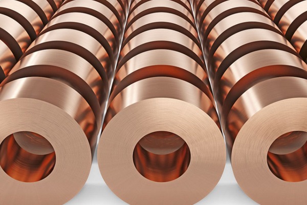
1. Kernvorteile von Kupfer als bevorzugtes Leiterplattenmaterial
1.1 Unerreichte elektrische Leistung
- Second only to silver in conductivity, the resistivity of 1.68 × 10⁻⁸ Ω·m ensures efficient signal transmission.
- Hervorragender Hochtonbereich: Behält die Impedanzcharakteristik trotz Skin-Effekten stabil bei.
- Hervorragende Strombelastbarkeit: 40 % höhere Strombelastbarkeit als Aluminium bei gleicher Querschnittsfläche.
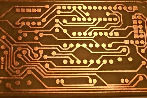
1.2 Außergewöhnliche Prozesskompatibilität
- Fähigkeit zum Präzisionsätzen: Unterstützt ultrafeine Spuren unter 3 mil.
- Mehrschichtige Laminierung: Entspricht dem Wärmeausdehnungskoeffizienten (CTE) von FR4’s.
- Vielseitige Oberflächenausführungen: Kompatibel mit allen gängigen Verfahren (ENIG/OSP/HASL).
1.3 Kosten-Wirksamkeits-Analyse
- Materialkosten: 1/50 des Preises von Silber und nur 1,2x Aluminium.
- Verarbeitungskosten: Ausgereifte Verfahren erzielen Erfolgsquoten von über 98 %.
- Wiederverwertbarkeit: Über 95 % Kupferrückgewinnungsrate aus Altplatten.
2. Technischer Wert von Kupfergießtechniken
2.1 Verbesserte elektromagnetische Verträglichkeit (EMV)
- Wirksamkeit der Abschirmung: Vollkupferguss reduziert die abgestrahlten Störungen um >15 dB.
- Signalrückleitungen: Bietet die kürzesten Rückwege für Hochgeschwindigkeitssignale.
- ImpedanzkontrolleBehält die Eigenschaften der Übertragungsleitung bei.
2.2 Verbessertes Wärmemanagement
- Wärmeleitfähigkeit: Outstanding 398W/(m·K) heat dissipation capability.
- Wärmespreizendes Design: Verhindert lokalisierte Hot Spots.
- Kühlung der Stromversorgungsgeräte: Kupferdicke im Vergleich zur Strombelastbarkeit:
| Kupferdicke (oz) | Leiterbahnbreite (mm) pro 1A |
|---|---|
| 1 | 0.4 |
| 2 | 0.2 |
| 3 | 0.13 |
2.3 Optimierung der mechanischen Festigkeit
- Biegefestigkeit: Erhöht die Steifigkeit des Substrats um >30%.
- Stabilität der Abmessungen: Widerstandsfähig gegen Verformung durch Temperatur- und Feuchtigkeitsschwankungen.
- Vibrationsfestigkeit: Obligatorisch für militärische Anwendungen.
3. Praktischer Leitfaden für die Gestaltung von Kupfergüssen
3.1 Vergleich von zwei grundlegenden Gießverfahren
Massiver Kupferguß
- Anwendungen: Leistungsebenen, Hochstrompfade
- Special treatment: Requires thermal relief slots (width ≥0.5mm)
- Typische Parameter:1-3oz Dicke, <30% Öffnungsverhältnis
Gitter Kupfer Gießen
- Beste Verwendung: Bereiche mit hochfrequenten Signalen
- Grid specifications: Line width/spacing ≥5mil
- Vorteile:Geringere thermische Belastung, 15 % weniger Gewicht
3.2 Normen für die Handhabung von Sonderzonen
- Antennenbereiche: 20 mm Abstand einhalten
- Unter BGA: Verwenden Sie kreuzförmige Pad-Verbindungen
- Brettkanten: Implement ≥3mm copper rings
3.3 Häufige Designfehler und Korrekturen
- Kupferne Inseln: Eliminieren Sie Durchkontaktierungen zur Erdung
- Scharfe Ecken: Replace with curved transitions (radius ≥3x trace width)
- Ungleichmäßige Wärmeabgabe: Implementierung von graduellen Kupferdickenabstufungen
- Impedanz-Fehlanpassung: Strenge Kontrolle der Toleranzen für die dielektrische Schichtdicke
- Fehler beim Löten: Optimieren Sie die Abmessungen der Lötmaskenöffnung
4. Entwicklungen an den Grenzen der Industrie
- Ultradünne Kupferfolien: Performance in 5G mmWave circuits (12μm thickness)
- Hybride Materiallösungen: Thermische Testdaten für Kupfer-Graphen-Verbundwerkstoffe
- 3D-gedruckte Kupferschaltungen: Präzisionsdurchbrüche in der LDS-Technologie
- Umweltfreundliche Verarbeitung: Fortschritte bei der cyanidfreien Kupferbeschichtung