Die Menschen stellen immer mehr komplexe elektronische Geräte her. Für diese Geräte sind 10-Lagen-Leiterplatten die beste Wahl für ihre Schaltungslayouts. Sie bieten eine bessere Routingdichte und Signalintegrität und können die Stromverteilung und die elektromagnetische Verträglichkeit bewältigen. Topfast bietet Lösungen für den Entwurf und die Konfiguration von 10-Lagen-Leiterplattenstapeln.Diese Lösungen helfen Unternehmen, die Leistung ihrer Schaltungen zu verbessern.
Inhaltsübersicht
Grundlegender Aufbau und Vorteile von 10-Lagen-Leiterplatten-Stapeln
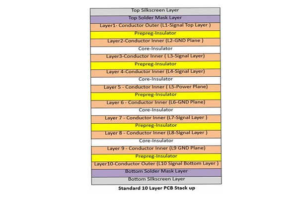
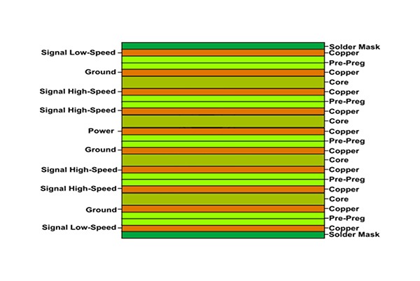
Standard-Stackup-Struktur
Eine typische 10-Lagen-Leiterplattenstapel verwendet die folgende mehrschichtige Architektur:
- Oberste Schicht (Signalschicht) – Platzierung von Bauteilen und Verlegung kritischer Signale
- Prepreg-Material – Zwischenschichtisolierung
- Internes Signal Schicht 1 – Sekundäres Signalrouting
- Kernmaterial – Bietet mechanische Stabilität
- Strom/Boden-Ebene 1 – Energieverteilung und Lärmschutz
- Prepreg-Material – Zwischenschichtisolierung
- Internes Signal Schicht 2 – Zusätzliches Signalrouting
- Kernmaterial – Bietet mechanische Stabilität
- Strom/Boden-Ebene 2 – Zusätzliche Stromverteilungsebene
- Untere Schicht (Signalschicht) – Signalverlegung und Komponentenmontage
Die wichtigsten Vorteile von 10-Schicht-Stapeln
- Erhöhte Design-Flexibilität: Mehr Ebenen ermöglichen komplexere Schaltungslayouts.
- Außergewöhnliche Signalintegrität: Dedizierte Signal- und Masseschichten reduzieren das Übersprechen.
- Optimierte Energieverteilung: Mehrere Leistungsebenen minimieren Spannungsabfall und Rauschen.
- Unterstützung für High-Density-Designs: Geeignet für BGAs und andere Fine-Pitch-Komponenten.
- Ausgewogene Kosteneffizienz: Ideales Gleichgewicht zwischen Leistung und Kosten.
Konfigurationsoptionen für 10-Lagen-Leiterplattenstapel
1. Standard-Konfiguration
Ein symmetrisches Design mit abwechselnden Signal- und Stromversorgungs-/Erdungslagen, geeignet für die meisten allgemeinen Anwendungen.
2.Mixed-Signal-Konfiguration
Trennt analoge und digitale Signalbereiche für verbesserte Signaltrennung und Rauschkontrolle.
3.Optimierte Hochgeschwindigkeits-Konfiguration
Speziell für Hochgeschwindigkeitssignale entwickelt, mit speziellen Signalebenen und verbesserten Referenzebenen.
4.Konfiguration der Energieintegrität
Mehrere Leistungsschichten optimieren das Stromverteilungsnetz (PDN) und reduzieren Spannungsschwankungen.
5.Eingebettete Kapazitätskonfiguration
Eingebettete Kapazitätsschichten verbessern die Entkopplung und reduzieren elektromagnetische Störungen.
Professionelle Gestaltungsrichtlinien und bewährte Praktiken
Management der Signalintegrität
- Physikalische Isolierung von Hochgeschwindigkeitssignalen von rauschempfindlichen Schaltungen.
- Verwenden Sie Erdungsschichten neben kritischen Signallagen, um Rückleitungen zu ermöglichen.
- Behalten Sie eine konsistente Impedanzkontrolle über alle Schichten hinweg bei.
Strategien zur Impedanzkontrolle
- Verwenden Sie professionelle Tools zur Impedanzberechnung, um die genauen Abmessungen der Leiterbahnen zu bestimmen.
- Berücksichtigen Sie Schwankungen der Dielektrizitätskonstante und der Dicke des Materials.
- Achten Sie auf einheitliche Leiterbahnbreiten, um Impedanzkontinuität zu gewährleisten.
Optimierung der Energieverteilung
- Implementieren Sie mehrschichtige Leistungsebenen, um die Impedanz zu verringern.
- Platzieren Sie Hochfrequenz-Entkopplungskondensatoren in der Nähe der Versorgungspins.
- Die Leistungssegmentierung nach dem Inselstil verhindert die Ausbreitung von Rauschen.
Überlegungen zum Wärmemanagement
- Sorgen Sie für einen ausreichenden Abstand für die Stromversorgungsgeräte (empfohlen >100 mils).
- Integrieren Sie thermische Durchkontaktierungen und Kupfer-Wärmeableitungsbereiche.
- Getrennte Bereiche mit hoher Wärmeentwicklung zur Vermeidung thermischer Kopplung.
Überlegungen zur Herstellung
- Verify the manufacturer’s capability to produce 10-layer boards.
- Klären Sie besondere Anforderungen (z. B. Impedanzkontrolle, blinde/vergrabene Durchkontaktierungen).
- Bewertung der Kostenauswirkungen komplexer Entwürfe.
Topfast verfügt über umfassende Erfahrung in der Herstellung von 10-Lagen-Leiterplatten und bietet seinen Kunden professionelle Designunterstützung und Produktionsdienstleistungen. Unser Entwicklungsteam zeichnet sich durch die Handhabung verschiedener komplexer Stapelanforderungen aus und stellt sicher, dass jede Leiterplatte die höchsten Leistungsstandards erfüllt.
Wenn Sie mehr über unsere Möglichkeiten zur Herstellung von 10-Lagen-Leiterplatten erfahren oder eine professionelle Designberatung wünschen, besuchen Sie unsere offizielle Website oder Kontakt zu unserem technischen Team.
Ein sorgfältig konzipierter 10-Lagen-Leiterplattenstapel bietet eine ideale Leistungsplattform für komplexe elektronische Geräte. Durch die sorgfältige Berücksichtigung von Signalintegrität, Stromverteilung und EMV-Anforderungen kann die Wahl eines erfahrenen Partners wie Topfast sicherstellen, dass Ihr 10-Lagen-Leiterplattenprojekt vom Design bis zur Produktion reibungslos verläuft und letztendlich leistungsstarke, zuverlässige und langlebige Leiterplattenprodukte liefert.