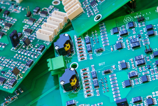
In the field of electronic manufacturing, the quality and efficiency of PCBA processing largely depend on the design and manufacturing standards of PCB boards. As a one-stop PCBA intelligent manufacturing provider, we understand the importance of adhering to industry best practices for product quality. This article details six core requirements for PCB boards in PCBA processing, helping you optimize production processes and enhance product reliability.
Table of Contents
PCB Material Selection
Material Properties Determine Application Scenarios
PCB substrate materials are fundamental factors affecting circuit performance. FR-4 fiberglass epoxy laminate is the preferred choice for most electronic products due to its excellent cost-performance ratio, featuring:
- Good mechanical strength
- Moderate dielectric constant
- High cost-effectiveness
Special Application Requirements
For high-frequency circuits or high-power devices, we recommend:
- Ceramic Substrates: Excellent high-temperature resistance (withstands above 300°C)
- Aluminum Substrates: Outstanding heat dissipation (thermal conductivity up to 2-4W/4W/mK)
Thickness Standards
The industry standard thickness is 1.6mm ±10%. Boards thinner than 1.0mm are prone to deformation during processing, affecting SMT placement accuracy.

Dimensional Tolerance Control
Machining Standards
PCB outline dimensional tolerances should be strictly controlled within ±0.1mm, which is critical for:
- Housing fit accuracy
- Connector alignment reliability
- Batch production consistency
Design Recommendations
Maintain at least 3mm of process edges on PCB borders to facilitate clamping and positioning in automated production lines.
Pad Design Specifications
Component Matching Principle
Pad design must precisely match component pin dimensions:
- 0603 package: Recommended pad size 0.8mm × 1.0mm
- SOIC package: Pads should extend 0.3-0.5mm beyond pins
Spacing Requirements
Minimum pad spacing standards:
- Standard components: ≥0.2mm
- BGA components: ≥0.15mm
BGA Design Key Points
For 0.5mm pitch BGAs, NSMD (Non-Solder Mask Defined) pad design is recommended, improving soldering reliability by approximately 30%.
Trace Design Standards
Current Carrying Capacity
Trace width vs. current (1oz copper thickness):
| Current (A) | Minimum Trace Width (mm) |
|---|---|
| 1 | 0.25 |
| 3 | 0.75 |
| 5 | 1.50 |
Spacing Specifications
Per IPC-2221 standards:
- Low-voltage circuits (≤30V): ≥0.1mm
- Medium-voltage circuits (30-100V): ≥0.6mm
- High-voltage circuits (≥100V): Calculate as 0.6mm/kV
Via Design Optimization
Hole Size Design Principles
Recommended hole size: 0.2mm larger than component pins:
- Standard through-hole components: 0.8-1.0mm hole size
- High-density designs: Minimum 0.3mm (laser drilling required)
Current Carrying Solutions
For high-current paths:
- Use multiple vias in parallel
- Increase via copper thickness (up to 2oz)
- Apply conductive epoxy filling
Surface Finish Technologies
Common Process Comparison
| Process Type | Thickness (μm) | Advantages | Application Scenarios |
|---|---|---|---|
| HASL | 1-25 | Low cost | Consumer electronics |
| ENIG | Ni3-5/Au0.05-0.1 | High flatness | Precision BGA |
| OSP | 0.2-0.5 | Eco-friendly | Short-term storage products |
Selection Recommendations
High-frequency signal circuits should use ENIG, reducing signal loss by approximately 15%.
Common Issues and Solutions
Production Challenge Countermeasures
- Soldering Defects: Optimize pad design + adjust reflow profile
- Short Circuits: Enhance AOI inspection + increase test coverage
- Impedance Control: Use high-frequency materials + strictly control trace width tolerance
Quality Assurance Measures
We provide:
- DFM (Design for Manufacturability) analysis services
- 3D PCB simulation verification
- 100% electrical testing
Conclusion: Optimizing PCB Design Enhances Overall Value
By following these PCB design specifications, customers can achieve:
✓ 20-30% improvement in production efficiency
✓ Defect rates reduced to <500ppm
✓ Approximately 25% longer product lifespan
We recommend involving PCBA manufacturing experts early in the product design phase to avoid costly late-stage modifications through collaborative design. Optimizing PCB design not only improves product reliability but also significantly reduces overall production costs, creating a competitive market advantage for your products.