In today’s rapidly evolving electronics industry, multilayer PCB prototyping has become a core part of the product development process. It serves not only as a touchstone for design validation but also as a key factor in seizing market opportunities. The challenge for every engineer and purchaser is how to achieve fast delivery and precise customization while ensuring quality.
Table of Contents
Core Value and Technical Challenges of Multilayer PCB Prototyping
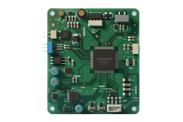
Multilayer PCB prototyping refers to the precise manufacturing of a small number of sample boards before mass production, used for functional testing, performance verification, and design optimization. Compared to single or double-sided boards, multilayer boards (especially those with six layers or more) achieve higher wiring density, better signal integrity, and stronger anti-interference capabilities through alternating conductive and insulating layers. They are widely used in communication equipment, high-end consumer electronics, automotive electronics, and industrial control applications.
However, increasing the number of layers also introduces significant technical challenges:
- High-Density Interconnect (HDI) Requirements: Modern electronic designs are trending toward miniaturization and high frequency/speed, demanding minimum trace width/spacing of 3 mil or even smaller, and laser blind via diameters as small as 0.1mm.
- Material Diversity: There is a need to flexibly select FR-4 high Tg materials, halogen-free materials, or high-frequency and high-speed materials (such as MEGTRON6, ROGERS) based on the application scenario.
- Reliability Requirements: Products must operate stably in harsh environments, imposing stringent standards on thermal management, impedance control, and long-term reliability.
Overcoming the Four Core Challenges
To complete multilayer PCB prototyping, the following four core challenges must be systematically addressed:
1. Layer-to-Layer Alignment Accuracy Control
As the number of layers increases, the cumulative alignment error between layers becomes a primary cause of scrap. Advanced manufacturers employ high-precision positioning systems and environmental temperature/humidity control to strictly maintain layer-to-layer alignment tolerance within ±25µm, enabling the realization of complex designs such as any-layer HDI.
2. Inner Layer Circuit Fabrication and Pattern Transfer
The inner layer circuitry is the backbone of a multilayer board. Fine lines, high Tg materials, and thin core layers are prone to wrinkling, misalignment, and uneven etching during processing. Adopting Laser Direct Imaging (LDI) technology instead of traditional film exposure significantly improves the alignment accuracy and line width uniformity of inner layer patterns.
3. Lamination Process Reliability
Lamination is the critical step of bonding multiple inner-layer cores and prepreg into a single entity. The challenges lie in controlling defects such as layer shifting, delamination, and resin voids.
- Solution: Develop a scientific lamination procedure, precisely controlling the heating rate, pressure profile, and vacuum level. For 6-layer boards, a symmetrical stack-up design (e.g., 3+1+3) is often used to prevent warping.
4. High-Precision Drilling and Hole Metallization
Thick boards and multiple stacked vias pose challenges like drill bit breakage, burrs, and drill smear during drilling. Micro vias and buried vias place extremely high demands on laser drilling technology.
- Solution:
- Mechanical Drilling: Use new drill bits and optimized parameters to tackle thick copper and thick boards.
- Laser Drilling: Used for processing micro vias of 0.1mm and below, offering high precision and good hole wall quality.
- Hole Metallization: Employ efficient desmear and electroless copper deposition processes to ensure clean hole walls and uniform copper coverage, guaranteeing the reliability of interlayer electrical connections.
Standardized Prototyping Flow and Key Process Analysis
An efficient and reliable multilayer PCB prototyping process is the guarantee of quality and speed. Its core steps can be summarized as follows:
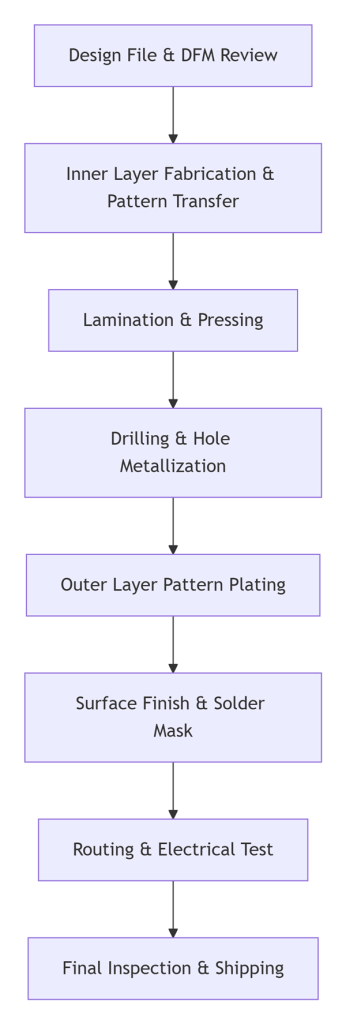
In-depth Analysis of Key Processes:
- Impedance Control: For high-speed signals, impedance matching is crucial. Engineers need to accurately calculate line width and dielectric thickness during the design phase, while manufacturers must strictly control the production process to ensure the final impedance deviation is within ±10% (or a stricter ±5% if required).
Surface Finish Selection: Different applications require different surface finish processes.
| Surface Finish | Advantages | Typical Applications |
|---|---|---|
| ENIG | High flatness, good solderability, oxidation resistance | BGA, precision components, high-frequency circuits |
| HASL (Lead-Free) | Low cost, strong solder joints | Consumer electronics, applications where extreme flatness is not critical |
| Immersion Tin | Environmentally friendly, suitable for press-fit connections | Specific industrial, communication fields |
| OSP | Lowest cost, preserves copper solderability | Low-complexity products, short storage life cycles |

Strategies for Fast Delivery and Manufacturer Selection
“Speed” is a core competitive advantage in multilayer PCB prototyping. Achieving fast delivery requires joint efforts from both the customer and the manufacturer.
Customer-Side Optimization Strategies:
- Design Standardization: Follow IPC standards and avoid non-standard hole sizes and trace widths.
- Provide Complete Data: Submit standard Gerber files, accurate BOM lists, and clear process requirements.
- Utilize DFM Analysis: Use the DFM (Design for Manufacturability) service provided by the manufacturer before production to identify and correct design flaws early.
Manufacturer Capability Assessment:
When selecting a prototyping manufacturer, consider the following dimensions:
- Technical Equipment: Do they possess advanced equipment like LDI, high-precision laser drilling machines, and automated AOI inspection systems?
- Process Maturity: Do they have stable mass production experience for 6-layer boards, HDI boards, and even high-layer count boards above 20 layers?
- Quality System: Are they certified under international quality standards like ISO9001, IATF16949?
- Delivery Guarantee: Do they clearly offer expedited prototyping services (e.g., 24 hours for 6-layer, 72 hours for high-layer count)? Is the production progress transparent and traceable?
Application Scenarios Summary and Future Trends
The success of multilayer PCB prototyping is ultimately reflected in the cutting-edge products it enables:
- Consumer Electronics: Mainboards for smartphones, AR/VR devices, pursuing miniaturization and any-layer HDI.
- Communication Equipment: 5G base stations, servers, requiring low-loss, high-frequency materials, and strict impedance control.
- Automotive Electronics: ADAS controllers, requiring high reliability, high-temperature resistance, and excellent thermal performance.
- Industrial and Medical: Industrial robots, medical imaging equipment, emphasizing long-term stable operation in complex environments.
Looking ahead, with the further development of AI, IoT, and automotive electronics, the requirements for multilayer PCB prototyping will continue to evolve toward higher density, higher frequency, higher reliability, and shorter development cycles.