
Table of Contents
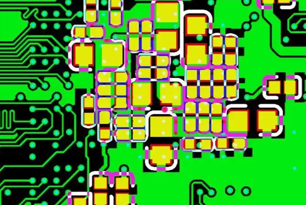
What is Via-in-Pad?
Via-in-Pad (VIP) technology essentially means placing vias directly inside component pads. Think of it this way: while traditional designs place vias next to pads, VIP allows vias to “reside” inside the pads themselves.
Why Use Via-in-Pad?
Application Scenario Comparison Table
| Application Scenario | Traditional Design Pain Points | VIP Solution |
|---|---|---|
| BGA Chips | Pins too dense, no space for vias | Vias are hidden under pads, saving space |
| High-Frequency Circuits | Long signal paths affect performance | Shorten paths, improve signal quality |
| Power Modules | Poor heat dissipation, chips overheat | Enhance heat dissipation through vias |
Real Case: The BGA package of a processor on a smartphone motherboard has a pin pitch of only 0.4mm – without VIP, routing would be impossible!
Two Core Processes: Resin Plugging vs. Electroplating Filling
Process Comparison Table
| Characteristic | Resin Plugging | Electroplating Filling |
|---|---|---|
| Cost | Medium | High |
| Difficulty | Relatively Easy | Difficult |
| Surface Flatness | Good (requires grinding) | Excellent |
| Thermal Conductivity | Average | Excellent |
| Application Scenarios | Standard BGA | High-end chips, high heat dissipation requirements |
Key Points for Resin Plugging Practice
Material Selection is Key:
High-quality resin = Low shrinkage rate + High Tg value + Matched CTE
If the resin shrinkage rate is too high, a “pitting effect” occurs – similar to road subsidence, causing pad surface depression and leading to soldering defects.
Process Control Points:
- Cleanliness: Contamination in holes? Absolutely not! Like a sterile operation in surgery
- Filling Pressure: Too high → resin overflow; Too low → incomplete filling
- Curing Curve: Rapid temperature rise causes bubbling, like controlling heat when baking
Insider Knowledge of Electroplating Filling Technology
High Equipment Requirements:
- Horizontal copper deposition equipment
- Pulse electroplating system
- Precision control software
Success Indicator: During cross-section inspection, the hole must be like a solid copper pillar with no voids!
“Pit Avoidance Guide” for the Design Phase
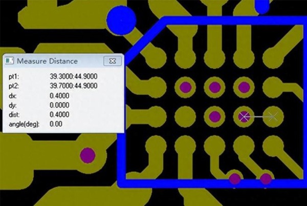
Golden Rules for Aperture Design
Recommended: 0.10mm laser via
Warning: Filling difficulty increases dramatically for holes >0.15mm!
Pad Size Calculation:
Pad diameter ≥ Hole diameter + 0.20mm
Example: For a 0.10mm hole diameter, the pad should be at least 0.30mm
Wisdom in Material Selection
- Base Material: Choose FR-4 TG170 or higher for high temperature resistance
- Copper Foil: Must be compatible with the electroplating process
- Early Communication: Don’t assume manufacturers can do everything!
Production Process
Manufacturing Process Flow
Drilling → Hole Metallization → Plugging/Filling → Surface Treatment → Inspection
Key Control Points
Drilling Stage:
- Control the “heat” properly for laser drilling
- Mirror-smooth hole walls are ideal
Plugging Stage Quality Checklist:
- Surface Flatness: Depression <25um
- Fill Rate: >95%
- Bubbles: Zero tolerance
- Cleanliness: No contamination
Quality Inspection
Comprehensive Inspection Methods
| Inspection Method | What to Check | Standard Requirements |
|---|---|---|
| Microsection Analysis | Internal structure | No voids, copper thickness meets standards |
| AOI Inspection | Surface defects | No depression, no contamination |
| X-Ray | Internal filling | No large-area voids |
| Electrical Test | Connection performance | 100% continuity test |
Reliability Test Items
- Thermal Stress Test: 288℃ solder pot immersion for 10 seconds, check for board delamination
- Temperature Cycling: -55℃ to 125℃ repeated testing, verify lifespan
- Thermal Shock Test: Instant switching between extreme cold and heat, test material adhesion
When Should You Use Via-in-Pad?
Recommended Application Scenarios
- Under BGA chips, especially with a pitch <0.8mm
- CPU/GPU power pins require good heat dissipation
- High-frequency differential signals require consistent impedance
- High-speed interfaces like HDMI, USB3.0
Use with Caution
- Cost-sensitive projects require trade-offs
- When the manufacturer’s process capability is insufficient
- When traditional designs suffice for standard pitch components
Summary
Via-in-Pad is a key technology for high-density PCB design, requiring close collaboration between design and manufacturing teams for successful implementation. Through appropriate process selection, rigorous quality control, and thorough reliability verification, its advantages in space savings and performance enhancement can be fully realized.