Table of Contents
PCB: The Core Carrier and Performance Cornerstone of AI Hardware
1.1 Foundational Support Role
Printed Circuit Boards (PCBs), serving as the “skeletal neural network” of electronic systems, play a key interconnection function within AI hardware architectures. In AI servers, edge computing devices, and intelligent terminals, high-performance PCBs are responsible for connecting GPU/TPU clusters, high-bandwidth memory (HBM), and high-speed interfaces, enabling efficient data flow.
1.2 Evolution of Technical Specifications
- Increased Line Density: PCB trace width/space in AI servers is evolving from the conventional 0.1mm towards 0.05mm, increasing routing density by 3-5 times.
- Increased Layer Count: Standard server PCBs typically have 12-16 layers, whereas AI training server PCBs commonly reach 20-38 layers, with complex backplanes even exceeding 40 layers.
- Breakthrough in Signal Rates: Upgrading from 56Gbps PAM4 to 112Gbps PAM4, meeting the demands of high-speed interfaces like PCIe 6.0 and 800G optical modules.
1.3 Material and Process Innovation
- Application of High-Frequency Materials: Low-loss materials like Rogers RO4350B and Panasonic MEGTRON6 (Dk≤3.5, Df≤0.003) become the preferred choice for AI hardware.
- Breakthrough in Microvia Technology: Laser drill hole diameters are shrinking from 150μm to 50μm, requiring layer-to-layer alignment accuracy of ≤50μm.
- Upgraded Thermal Solutions: Innovative cooling technologies such as embedded copper blocks, thermal via arrays (reducing thermal resistance by 40%), and metal core substrates.
AI Technology Reshaping the Entire PCB Design and Manufacturing Process
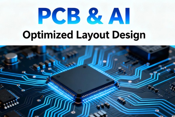
2.1 Intelligent Design Automation
(1) Layout and Routing Optimization
- AI-Driven Tools: Tools like Cadence Allegro X AI and Zuken CR-8000 achieve a 10x improvement in design efficiency.
- Intelligent Routing Algorithms: Optimize differential pair routing, impedance matching, and power distribution networks through reinforcement learning.
- Real-time Simulation Analysis: Tools like Sigrity X Aurora enable real-time signal integrity (SI) and power integrity (PI) analysis.
(2) Multi-Physics Co-design
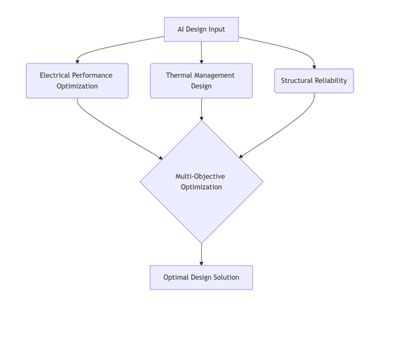
2.2 Intelligent Manufacturing and Quality Control
(1) Intelligent Inspection Systems
- Machine Vision Inspection: AOI systems based on deep learning achieve >99.5% defect recognition accuracy and <0.1% missed detection rate.
- Predictive Maintenance: Predicts failures in key equipment like laser drills and exposure machines by analyzing equipment data.
(2) Process Optimization
- Intelligent Parameter Adjustment: AI monitors etching and plating process parameters in real-time, automatically compensating for process variations.
- Yield Prediction: Establishes yield prediction models based on production data to identify potential quality issues early.
2.3 Supply Chain and Operations Management
- Demand Forecasting: Accurately predicts PCB demand changes through historical data and market trend analysis.
- Intelligent Production Scheduling: Multi-objective optimized scheduling considering equipment status, delivery requirements, and process characteristics.
- Inventory Optimization: Dynamic safety stock models reduce capital occupancy while ensuring production continuity.
Technical Challenges and Breakthrough Paths
3.1 Current Technical Bottlenecks
| Challenge Area | Specific Problem | Impact Level |
|---|---|---|
| High-Density Interconnect (HDI) | Consistency in sub-50μm microvia processing | ⭐⭐⭐⭐⭐ |
| Signal Integrity | Channel loss control ≤0.15dB/in at 112Gbps | ⭐⭐⭐⭐ |
| Thermal Management | Cooling demand for AI chips above 3kW | ⭐⭐⭐⭐ |
| Material Limitations | Performance gap in domestic high-frequency materials | ⭐⭐⭐ |
3.2 Key Technological Breakthroughs
(1) Processing Technology Innovation
- Ultra-Fine Line Processing: Using picosecond UV lasers + LDI direct imaging technology, achieving trace width accuracy of ±2μm.
- Via Filling Plating Technology: Pulse plating + special additives achieve defect-free filling of micro blind vias.
- Lamination Process Optimization: Low CTE materials + intelligent temperature and pressure control reduce interlayer misalignment.
(2) Design Methodology Innovation
Traditional Flow: Requirements Analysis → Manual Layout → Simulation Verification → Iterative Modification
AI-Enhanced Flow: Intelligent Requirements Parsing → Automatic Layout & Routing → Real-Time Multi-Physics Simulation → Intelligent Optimization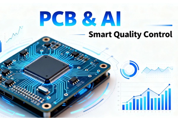
Industry Ecosystem and Future Trends
4.1 Evolving Market Landscape
- Global Market Size: The AI-specific PCB market is projected to reach 48 billion RMB by 2025, with a CAGR of 28%.
- Domestication Process: Domestic companies’ market share in server PCBs increased from 15% in 2020 to 35% in 2023.
- Technology Catch-up: Accelerating breakthroughs in high-end areas like 108+ layer ultra-high-layer boards and IC substrates.
4.2 Innovative Application Scenarios
(1) Heterogeneous Integration & Advanced Packaging
- 2.5D/3D Packaging: Co-design of silicon interposers, TSV technology, and high-density PCBs.
- Chiplet Architecture: Multi-chip modules require more complex substrate design and signal interconnection solutions.
(2) Emerging AI Hardware Forms
- Photonics Computing Interconnect: Photoelectric hybrid PCBs meet the interconnection needs of optical computing chips.
- Neuromorphic Hardware: Brain-inspired chips require three-dimensional wiring technology.
4.3 Technology Development Roadmap
Short Term (2024-2025):
- Improve the AI design tool ecosystem, achieving full-process design intelligence.
- Breakthrough in 5μm trace width/space processing technology.
- Increase yield for 112Gbps channels to over 95%.
Medium Term (2026-2028):
- Practical application of 3D printed wiring technology.
- Large-scale application of glass substrates and ceramic substrates.
- Maturation of 224Gbps transmission technology.
Long Term (2029+):
- Molecular-level self-assembling circuit technology.
- Quantum computing interconnection solutions.
- Bio-degradable PCB materials.
Collaborative Development Value and Outlook
The deep integration of PCB and AI is creating significant synergistic value:
- Technical Level: AI drives upgrades in PCB design and manufacturing capabilities, while advanced PCBs support the continuous improvement of AI computing power.
- Industry Level: Forms a positive cycle of “hardware innovation – algorithm optimization – application deployment”.
- Economic Level: Reduces the cost of AI hardware, accelerating the popularization and application of AI technology.
In the future, with the joint progress of materials science, precision manufacturing, and artificial intelligence technologies, PCBs will develop towards higher density, lower loss, and greater intelligence, providing a solid hardware foundation for next-generation AI systems. Simultaneously, AI technology will play a greater role in the entire PCB design, manufacturing, and testing workflow, promoting the digital and intelligent transformation of the electronics manufacturing industry.