Table of Contents
Detailed Methods and Considerations for PCB Mounting Hole Installation
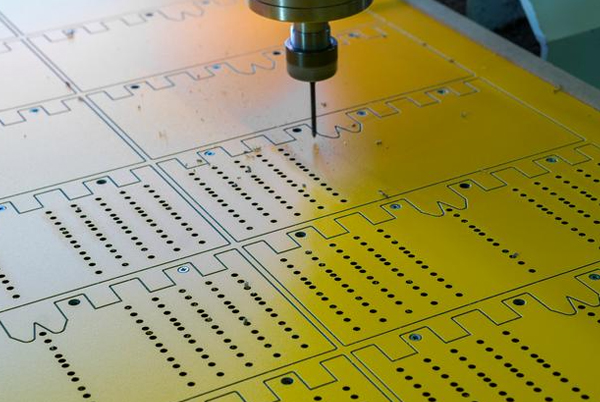
In PCB design, proper mounting hole installation is crucial for ensuring precise alignment during manufacturing, assembly, and usage. Mounting holes serve not only as reference points for production fixtures but also as important benchmarks for future maintenance.
Detailed Design Phase Considerations
When using professional PCB design software (such as Altium Designer, Eagle, or KiCad), mounting hole design requires systematic planning:
- Location Selection: Typically placed at the four corners of the PCB, at least 3mm from the board edge. For irregularly shaped PCBs, additional central mounting holes may be needed. Industry standards recommend using at least three non-collinear mounting holes for stability.
- Hole Size Determination: Standard hole sizes range from 1.0–3.0mm. Considerations include:
- Diameter of alignment pins used in assembly
- PCB thickness (thicker boards require larger holes)
- Environmental vibration factors (high-vibration environments need tighter fits)
- Tolerance Setting: Typical mounting hole tolerance is ±0.05mm, with high-precision applications requiring ±0.02mm. Ensure clear labeling in Gerber files.
Key Pre-Manufacturing Checks
Before submitting designs to manufacturers, verify the following:
- Distance from Board Edge: Ensure mounting hole centers are at least 3mm from the edge to prevent breakage during machining.
- Clearance from Other Components: No components or traces should be within 3mm of mounting holes.
- Non-Plated Hole Indication: Most mounting holes should be non-plated and must be explicitly noted.
- Layer Symmetry: For multilayer boards, mounting hole positions must account for layer symmetry to avoid warping.
Common Mounting Hole Types and Applications
- Round Mounting Holes: Most common, suitable for general applications.
- Slotted Mounting Holes: Allow slight positional adjustment, ideal for assemblies with different thermal expansion coefficients.
- Countersunk Mounting Holes: Facilitate easy pin insertion, ideal for quick assembly.
- Plated Mounting Holes: Used when an electrical connection is required, but increases cost.
In-Depth Analysis and Selection of PCB Connection Methods
Detailed Implementation of Standard Pin Headers
Standard pin headers are a cost-effective choice, especially for small-to-medium production runs:
Key Implementation Points:
- Pin spacing is typically 2.54mm (0.1 inch) or 2.0mm.
- Dual-row headers are recommended for enhanced stability.
- PCB pads should be 0.2–0.3mm larger than the pin diameter.
- Adequate support pads on the reverse side prevent detachment.
Advantages:
- Low cost, easy manual soldering.
- Reliable connections with low contact resistance.
- Simple repair and replacement.
Limitations:
- Occupies more PCB space.
- Unsuitable for high-frequency signal transmission.
- May loosen in high-vibration environments.
Professional Considerations for PCB Edge Connectors
PCB edge connectors (gold finger connectors) are ideal for frequent plugging/unplugging or modular designs:
Design Specifications:
- The gold finger length should exceed the contact area by 2–3mm.
- Gold finger thickness is typically 30–50µm.
- Edge chamfering (recommended 30–45 degrees).
- Non-contact areas require solder mask application.
Performance Optimization:
- Increase grounding fingers to reduce EMI.
- Place ground lines adjacent to critical signal lines.
- Include stress relief slots at finger ends.
Maintenance Tips:
- Clean contacts regularly with specialized cleaners.
- Avoid excessive plugging/unplugging (typical lifespan: 500–1000 cycles).
- Store in anti-oxidation bags when unused.
5 Common Issues and Professional Solutions
Issue 1: Mounting Hole Misalignment Causing Assembly Difficulties
Root Causes:
- Discrepancies between design files and Gerber outputs.
- Accumulated manufacturing tolerances.
- Mismatched coefficients of thermal expansion (CTE).
Solutions:
- Add fiducial markers for alignment assistance.
- Select higher-precision manufacturers (e.g., IPC-A-600 Class 3).
- Use compensation algorithms in NC drilling programs.
- Consider CTE-compatible materials.
Issue 2: Connector Contact Failure
Symptoms:
- Intermittent signal loss.
- Unstable contact resistance.
- Increased failure rates at high temperatures.
Troubleshooting Steps:
- Clean contacts (use isopropyl alcohol and a lint-free cloth).
- Check pin/connector spring tension (should meet MIL-STD-1344).
- Measure contact resistance (should be <50mΩ).
- Upgrade plating material if necessary (gold outperforms tin).
Issue 3: Connection Failure in High-Vibration Environments
Preventive Measures:
- Use latching connectors (e.g., Molex Micro-Fit 3.0).
- Add mechanical fasteners (screws + washers).
- Replace standard pins with threaded variants.
- Apply epoxy adhesive (select appropriate viscosity).
Issue 4: Excessive Gold Finger Wear
Lifespan Extension Methods:
- Use hard gold plating (2–5% cobalt content).
- Increase the number of fingers to distribute wear.
- Optimize insertion/removal guides.
- Control insertion force (use specialized tools).
Issue 5: Poor High-Frequency Signal Integrity
Improvement Strategies:
- Use impedance-matched connectors.
- Minimize connection lengths.
- Increase ground pins (at least 20% of total).
- Use differential signaling.
- Add EMI shielding gaskets.
Professional Summary
The selection of PCB mounting holes and connection methods has a direct impact on product reliability, manufacturability, and serviceability. Systematic design and strict process controls can significantly enhance overall electronic product quality.
Key Takeaways:
- Mounting holes should follow the “3-2-1” principle: restrict three translational and two rotational degrees of freedom.
- Connector selection must account for environmental factors: temperature, humidity, vibration, and corrosive gases.
- Gold finger layouts should use “staggered lengths” to ensure proper power sequencing.
- For high-frequency connections, prefer press-fit over soldered interfaces.
- Maintain connector lifespan records and implement preventive replacement schedules.
Latest Reading Recommendations
- The Ultimate Guide to HDI PCB Stack-up Design: From Basic Structures to Advanced Optimization Strategies
- Detailed Explanation of PCB V-Cut Panelization Technology
- PCB Assembly Design Guide
- How Flying Probe and Adapter Testing Are Reshaping PCB Quality Control Standards
- Mastering PCB Signal Integrity