Table of Contents
Surface Mount Devices (SMD): Comprehensive Technical Overview
Definition and Evolution
SMD (Surface Mounted Devices) represent a critical category within SMT (Surface Mount Technology) components. In the early stages of PCB manufacturing, through-hole assembly was entirely manual. While initial automation could handle simple pin components, complex parts still required manual placement before reflow soldering.
Primary SMD Classifications
- By Physical Form:
- Rectangular chip components
- Cylindrical chip components
- Composite chip components
- Special-shaped components
- By Functional Category:
- Interconnect Components:
- Function: Provide mechanical/electrical connection/disconnection
- Examples: Board-to-board connectors, FPC connectors
- Key Feature: Must utilize surface-mount contacts
- Active Components:
- Definition: Control voltage/current to produce gain/switching in circuits
- Characteristics: Require external power, alter fundamental properties
- Examples: ICs, transistors, diodes
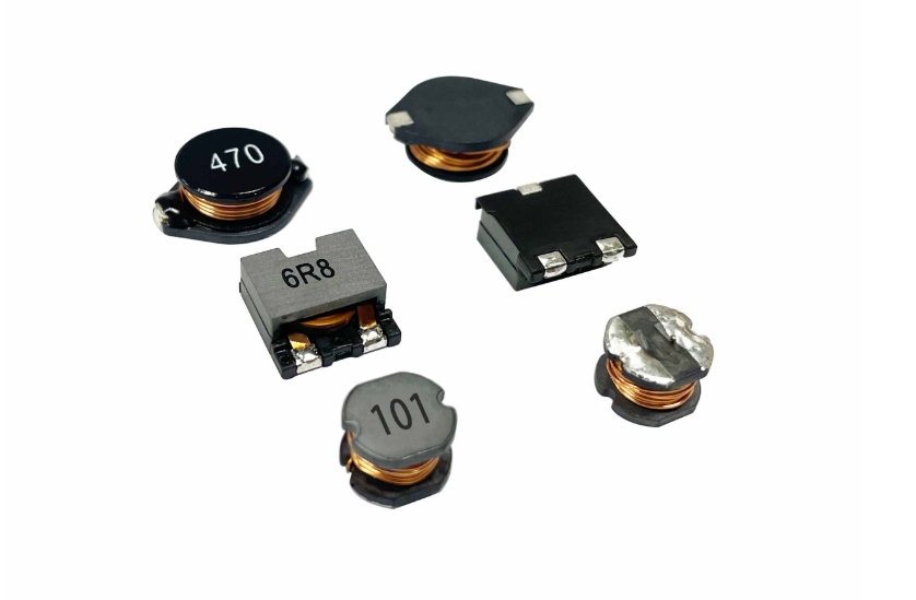
- Passive Components:
- Definition: Provide consistent, repeatable responses to signals
- Characteristics: No external power required
- Examples: Resistors, capacitors, inductors
- Odd-form Components:
- Definition: Non-standard geometric configurations
- Assembly: Typically requires manual placement
- Examples: Transformers, hybrid circuits, electromechanical switches
IC Package Types
- SOP (Small Outline Package)
- SOJ (Small Outline J-lead)
- PLCC (Plastic Leaded Chip Carrier)
- LCCC (Leadless Ceramic Chip Carrier)
- QFP (Quad Flat Package)
- BGA (Ball Grid Array)
- CSP (Chip Scale Package)
- FC (Flip Chip)
- MCM (Multi-Chip Module)
Standardized Specifications
| Component Type | Size Specifications | Notable Features |
|---|---|---|
| Chip R/C/L | 0201,0402,0603,0805,1206,1210,2010 | ±1% tolerance available |
| Tantalum Capacitors | TANA, TANB, TANC, TAND | Polarized, high capacitance |
| Transistors | SOT23,SOT143,SOT89 | Various pin configurations |
| MELF Components | Diodes, resistors | Cylindrical form factor |
| SOIC ICs | SOIC08-32 | 1.27mm pin spacing |
| QFP ICs | Various pin counts | 0.4-1.0mm pitch options |
| BGA Packages | 1.27,1.00,0.80mm array | High I/O density |
| CSP Packages | <0.50mm pitch | Chip-size packaging |
Special Note: Sauter Mean Diameter (SMD)
In spray nozzle applications, SMD refers to the diameter of a sphere that has the same volume/surface area ratio as the entire droplet population. This measurement is particularly important for:
- Fuel injection systems
- Coating applications
- Aerosol generation
Calculation methods include:
- Arithmetic mean diameter
- Geometric mean diameter
- Sauter mean diameter (most widely used)
This standardized approach allows for precise characterization of droplet size distributions in various industrial applications.
Key Advantages of SMT Technology
- Ultra-High Density Integration
- 90% reduction in component size (compared to traditional DIP components)
- Typical application results:
✓ 40-60% reduction in end product volume
✓ 60-80% reduction in overall weight
✓ 300%+ improvement in PCB area utilization
- Exceptional Reliability Performance
- Solder defect rate <0.02% (IPC-A-610 Class 3 standard)
- Enhanced mechanical properties:
✓ 10x improvement in vibration resistance
✓ 5x better shock resistance
✓ MTBF extended to 50,000 hours
- Superior Electrical Characteristics
- Optimized high-frequency performance:
✓ Parasitic inductance reduced to 0.1nH level
✓ Parasitic capacitance controlled within a 0.01pF range - Improved EMC performance:
✓ 30dB reduction in electromagnetic interference
✓ 40% better RF noise suppression
- Intelligent Manufacturing Benefits
- Automated production efficiency:
✓ Placement speed up to 200,000 CPH
✓ Line changeover time reduced to 15 minutes - Comprehensive cost benefits:
✓ 30-50% lower production costs
✓ 45% improvement in material utilization
✓ 40% energy savings
✓ 70% reduction in labor requirements
- Green Manufacturing Features
- Environmental benefits:
✓ Lead content compliant with RoHS 2.0
✓ 60% reduction in waste generation
✓ 35% lower energy consumption - Sustainable development:
✓ 50% higher product recyclability
✓ 40% smaller carbon footprint
Technology Comparison Data:
| Metric | Traditional THT | SMT | Improvement |
|---|---|---|---|
| Component density (pcs/cm²) | 2-4 | 10-16 | 400% |
| Production cycle (days) | 7-10 | 2-3 | 70% |
| Solder joint yield | 98.5% | 99.98% | 1.5% |
| Cost per unit area | $1.2/cm² | $0.6/cm² | 50% |
Note: Data based on industry benchmarks. Actual results may vary by application. SMT technology continues to advance toward 0201/01005 micro-components and 3D stacked packaging, driving ongoing innovation in electronics manufacturing.
PCB Layout for Surface Mounted Components
1. Pad Design Specifications
Two primary pad configurations exist for surface mount devices:
- NSMD (Non-Solder Mask Defined)
- Preferred configuration for most applications
- Advantages:
✓ 15% better copper etching control
✓ 30% reduction in stress concentration points
✓ Improved solder joint reliability - SMD (Solder Mask Defined)
- Used in specific high-density applications
- Requires tighter process controls
2. Copper Thickness Recommendations
- Optimal copper thickness: <30μm (1oz)
- Thinner copper provides:
✓ 20% greater standoff height
✓ Better solder joint formation
✓ Reduced thermal stress during reflow - For >30μm copper:
- Requires solder paste volume adjustment
- May need a modified reflow profile
3. Connection Design Rules
- Trace width between NSMD pads:
- Maximum: 2/3 of the pad diameter
- Recommended: 1/2 of the pad diameter
- Pad-via structures:
- Must use NSMD configuration
- Ensures sufficient solderable area
- Maintains 100% solder wettability
4. Surface Finish Options
| Finish Type | Thickness | Key Considerations |
|---|---|---|
| OSP | 0.2-0.5μm | Best for fine-pitch components |
| ENIG | Ni 3-5μm/Au 0.05-0.1μm | Avoid >0.5μm Au to prevent brittleness |
| HASL | Not recommended | Poor co-planarity for fine-pitch |
5. Critical Layout Practices
- Symmetrical Trace Routing
- Balance X/Y direction traces
- Prevents component rotation during reflow
- Maintains proper soldering alignment
- Thermal Relief Design
- Use spoke connections for ground pads
- Ensures even heat distribution
- Prevents tombstoning
- Solder Mask Considerations
- Clearance: 50μm minimum around pads
- Avoid mask-defined pads unless necessary
- Component Orientation
- Align similar components in the same direction
- Facilitates automated inspection
- Improves soldering consistency
Implementation Example:
For a 0402 component (1.0×0.5mm):
- NSMD pad size: 0.6×0.3mm
- Trace width: 0.2mm (max)
- Solder mask opening: 0.7×0.4mm
- Pad-to-pad spacing: 0.4mm
Note: These guidelines apply particularly to high-reliability applications, including automotive, medical, and aerospace electronics. Always verify with your PCB manufacturer’s capabilities before finalizing designs.
Difference between SMD and SMT assembly
Core Concept Definitions
- SMD (Surface Mount Devices)
- Technical definition: Miniaturized electronic components compliant with JEDEC standards
- Typical package types:
✓ Basic components: 0201/0402/0603 CHIP elements
✓ ICs: QFP (0.4mm pitch), BGA (0.5mm ball pitch), CSP, etc.
✓ Special devices: Leadless packages like QFN, LGA
- SMT (Surface Mount Technology)
- Process scope: Complete manufacturing flow from solder paste printing to reflow soldering
- Technological evolution:
1st Gen (1980s): Basic chip component placement
2nd Gen (1990s): Fine Pitch components (0.65mm pitch)
3rd Gen (2000s): 01005 micro-components/0.3mm pitch BGA
II. Comparative Technical Characteristics
| Feature Dimension | SMD | SMT |
|---|---|---|
| Essential Nature | Physical components | Manufacturing process system |
| Size Advantage | 90% smaller than through-hole | 200,000 placements/hour |
| Typical Application | High-density IC packaging | Fully automated production |
| Quality Metrics | Solderability, heat resistance | Solder joint yield (>99.99%) |
| Development Trend | 3D packaging/heterogeneous integration | Smart factory/digital twin |
Collaborative Working Mechanism
- Technical Complementarity
- SMD provides hardware foundation: Modern 0402 components measure just 0.4×0.2mm
- SMT enables manufacturing breakthroughs: Latest placers achieve ±15μm@3σ accuracy
- Process Optimization Path
- Design synergy: DFM rules ensure SMD manufacturability
- Material innovation: Low-temperature solder for heat-sensitive SMDs
- Equipment upgrades: 3D SPI inspects 01005 component solder paste
- Performance Enhancement
- Space utilization: 300% improvement over THT
- Production cost: 40-60% reduction
- Reliability: MTBF extended to 50,000 hours
Integrated Applications in Modern Electronics Manufacturing
- Miniaturization Implementation
- Smartphones: Adopt 0.25mm pitch CSP packages
- Wearables: Utilize flexible SMDs + roll-to-roll SMT
- High-Frequency Applications
- 5G base stations: High-frequency SMDs with vacuum reflow
- Automotive radar: Special placement processes for 77GHz components
- High-Reliability Fields
- Aerospace electronics: Radiation-resistant SMDs + selective soldering
- Medical devices: Biocompatible SMDs + low-temperature SMT
Note: Per IPC-7351 standards, modern SMT lines must accommodate full-range SMD placement from 01005 to 50×50mm BGA. Their collaborative development is driving electronics manufacturing toward sub-0402 micro-components and 3D heterogeneous integration.
Micro SMD Surface Mount Technology Operation Specifications
Standard Operating Procedures
- Solder Paste Printing Phase
- Laser-cut stencil (thickness 0.1-0.15mm)
- Printing parameter controls:
✓ Squeegee pressure: 5-10N/cm²
✓ Printing speed: 20-50mm/s
✓ Separation speed: 0.5-1.0mm/s - 3D SPI inspection (10μm resolution)
- Component Placement Phase
- Equipment requirements:
✓ Placement accuracy: ±25μm @3σ
✓ Minimum placement component: 01005 (0.4×0.2mm) - Feeding system:
✓ EIA-481-1 compliant tape packaging
✓ Compatible with 8mm/12mm/16mm reels
- Reflow Soldering Phase
- Temperature profile control:
✓ Preheat slope: 1-3°C/s
✓ Peak temperature: 235-245°C (lead-free)
✓ Time above liquidus: 60-90s - Nitrogen protection (O₂<1000ppm)
Technical Advantage Analysis
| Advantage Dimension | Technical Implementation | Performance Metric |
|---|---|---|
| Standardized Packaging | EIA-481 tape packaging | 40% improved loading efficiency |
| Equipment Compatibility | Supports 0402-1206 full-size components | <15min changeover time |
| Process Stability | Six Sigma process control | CPK≥1.67 |
| Quality Reliability | Solder void rate <15% | First-pass yield >99.5% |
Key Control Points
- ESD Protection
- Work surface resistance: 10⁶-10⁹Ω
- Operators must wear wrist straps
- Humidity Control
- MSD component storage: ≤10%RH (with desiccant)
- Workshop environment: 40- 60% RH
- Process Validation
- First article inspection:
✓ 100% polarity verification
✓ Solder paste thickness measurement (±10% tolerance) - Process sampling:
✓ X-ray inspection every 2 hours (for BGA)
✓ Cross-section analysis every 4 hours
Note: For ultra-micro components below 0201 size, vacuum pick-up devices (vacuum ≥80kPa) and micro vision alignment systems (5μm resolution) are recommended. All process parameters must comply with IPC-A-610 Class 3 standards.