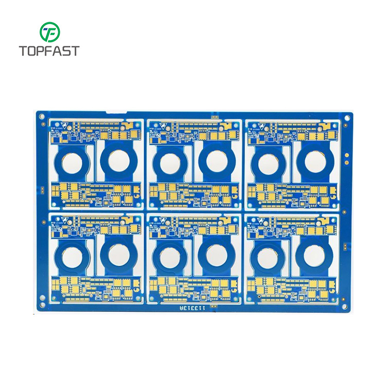
A quad-layer PCB circuit board is a multilayer circuit board that usually consists of an inner signal layer, an inner power layer, an outer signal layer, and an outer part mounting layer. Compared to single-sided and double-sided PCB circuit boards, quad-layer PCB circuit boards offer higher integration, smaller size, and more stable performance because it can pass power in the inner power layer (a layer not found on ordinary PCB circuit boards), thus reducing interference and noise and ensuring circuit stability.
Table of Contents
Technical Specifications of 4 Layer PCB Boards
Basic Structure
A 4-layer PCB adopts the classic “signal-power-ground-signal” stack-up configuration:
- Top Layer: Component mounting and surface routing
- Inner Layer 1: Signal transmission layer (priority for high-frequency signals)
- Inner Layer 2: Power plane (Power Plane)
- Bottom Layer: Signal layer and soldering surface
Core Advantages Comparison
| Performance Metric | Double-Layer PCB | 4-Layer PCB | Improvement |
|---|---|---|---|
| Routing Density | 2-4 lines/cm | 8-12 lines/cm | 300% |
| Signal Integrity | 60-80Ω impedance variation | ±5% impedance control | 5x better |
| Power Noise | 50-100mV | <10mV | 90% reduction |
| EMC Performance | Requires additional shielding | Built-in shielding layers | Complies with Class B |
Typical Applications
- High-Speed Digital Circuits
- Features: Clock frequencies above 100MHz
- Implementation: Complete return paths via inner ground planes
- Example: ARM processor boards (6-layer HDI with blind/buried vias)
- Analog-Mixed Systems
- Solution: Separate digital/analog power supplies
- Layout: Analog signals on top layer + digital signals on inner layers
- Performance: Crosstalk < -60dB @1GHz
- Power Electronics Design
- Configuration: 2oz thick copper power plane
- Capability: Current density up to 10A/mm²
- Thermal Management: Via arrays for heat dissipation
Manufacturing Key Points
- Lamination Control
- Dielectric thickness: 0.2mm ±5%
- Copper weight options: 1oz / 2oz
- Alignment accuracy: ≤50μm
- Via Design
- Through-hole: 0.3mm/0.6mm (hole diameter/pad)
- Blind vias: L1-L2 or L3-L4
- Buried vias: L2-L3 (requires laser drilling)
- Impedance Control
- Microstrip: 50Ω ±10% (outer layers)
- Stripline: 100Ω differential (inner layers)
- Verification: TDR (Time Domain Reflectometry) testing
Selection Guidelines
- Recommended Use Cases
- Operating frequency ≥50MHz
- Component count ≥100
- BGA packages (pitch ≤0.8mm)
- Requires 4+ power domains
- Cost Optimization
- Standard FR4 material (TG≥130℃)
- Minimum trace/space: 4mil/4mil
- Avoid blind/buried vias
Note: Modern 4-layer PCBs support 3mil trace/space with 0.25mm microvias, achieving routing density comparable to 6-layer boards. Per IPC-2221B standards, 4-layer PCBs can achieve a 10-year lifespan (industrial-grade applications).

Comprehensive Manufacturing Process of 4 Layer PCB Boards
Design Engineering Phase
- EDA Design Verification
- Professional tools: Cadence Allegro/Mentor Xpedition
- Signal integrity analysis (HyperLynx)
- Output: Gerber 274X format production files
- Key parameters:
✓ Minimum trace/space: 3/3mil
✓ Impedance control: ±10%
✓ Via count: ≥2000/m²
Material Preparation & Processing
- Copper Clad Laminate Selection
- Standard FR-4 (TG150)
- Copper thickness options: 1/2oz adjustable
- Dimensional tolerance: ±0.1mm
- Precision Drilling
- Equipment: 6-axis CNC drilling machine
- Accuracy:
✓ Hole position deviation: ≤25μm
✓ Hole diameter tolerance: ±50μm - Typical parameters:
✓ Spindle speed: 150krpm
✓ Panel stack thickness: ≤2.4mm
Multilayer Lamination Process
- Layer Stackup
| Layer | Designation | Thickness (mm) | Copper Weight | Primary Function |
|---|---|---|---|---|
| Top | Signal Layer (L1) | 0.035 ±0.005 | 1 oz | Component placement & routing |
| Inner | Power Plane (L2) | 0.50 ±0.05 | 2 oz | Power distribution & decoupling |
| Inner | Ground Plane (L3) | 0.50 ±0.05 | 2 oz | Signal return path & EMI shielding |
| Bottom | Signal Layer (L4) | 0.035 ±0.005 | 1 oz | Secondary routing & soldering |
2. Lamination Parameters
- Temperature: 180±5℃
- Pressure: 300±50psi
- Duration: 90±10 minutes
- Vacuum level: ≤10mbar
Pattern Transfer Technology
- LDI Exposure
- Resolution: 20μm
- Alignment accuracy: ±15μm
- Capacity: 50 panels/hour
- Circuit Etching
- Etch factor: ≥3:1
- Undercut control: ≤10%
- Copper thickness uniformity: ±5%
Plating & Surface Finishes
- Hole Metallization
- Electroless copper: 0.5-1μm
- Electroplated copper: 25±5μm
- Hole wall pull strength: ≥1.0N/mm
2. Surface Finish Options
| Surface Finish | Technical Specification | Thickness Range | Key Characteristics | Recommended Applications | Shelf Life | IPC Standard |
|---|---|---|---|---|---|---|
| ENIG (Electroless Nickel Immersion Gold) | Ni: 3-5μm Au: 0.05-0.1μm | Ni: 120-200μin Au: 2-4μin | – Excellent flatness – Good solderability – Aluminum wire bondable | – BGA packages – Fine-pitch components (<0.5mm) – Connectors | 12 months | IPC-4552 |
| OSP (Organic Solderability Preservative) | 0.2-0.5μm | 8-20μin | – Cost-effective – Lead-free compatible – Simple process | – Consumer electronics – General SMT assembly – High-volume production | 6 months | IPC-4555 |
| Immersion Tin | 0.8-1.2μm | 30-50μin | – Excellent solderability – Flat surface – Suitable for press-fit | – Automotive electronics – High-reliability applications – RF/microwave circuits | 9 months | IPC-4554 |
Quality Verification System
- Electrical Testing
- Flying probe test:
✓ Test speed: 200 points/sec
✓ Minimum pitch: 4 mil - Impedance test:
✓ TDR resolution: 5ps
✓ Test points: ≥5/impedance line
- Visual Inspection
- AOI:
✓ Resolution: 10μm
✓ Defect detection rate: ≥99.7% - Microsection analysis:
✓ Sampling frequency: 1/100m²
✓ Inspection items: 20+ parameters
Special Process Controls
- Impedance Control
- Microstrip: 50Ω±5%
- Stripline: 100Ω±7%
- Differential pairs: ±8%
- Thermal Management
- Thermal vias: 0.3mm diameter
- Distribution density: 25/cm²
- Copper thickness option: 2oz
Note: This process complies with IPC-6012 Class 3 standards, suitable for high-reliability applications like automotive electronics and industrial controls. Modern 4-layer PCB manufacturing can achieve 3mil trace/space with laser drilling technology, delivering HDI-like routing density.

Design and Advantages Analysis of 4-Layer PCB Stackup Structure
Basic Structure and Layer Configuration
A 4-layer printed circuit board (PCB) adopts a multi-layer composite structure, primarily consisting of the following functional layers:
- Signal Layers: Including the Top Layer and Bottom Layer, responsible for routing various signal traces.
- Power Layer (Power Plane): Provides stable power distribution to circuit components.
- Ground Layer (Ground Plane): Establishes the system reference potential and provides electromagnetic shielding.
Two common stackup configurations are widely used:
Option A: Top Layer → Power Layer → Ground Layer → Bottom Layer
- Features: Tight coupling between power and ground planes, forming an effective planar capacitance, particularly suitable for high-frequency circuit design.
Option B: Top Layer → Ground Layer → Power Layer → Bottom Layer - Features: The ground layer provides close shielding for signal layers, significantly reducing crosstalk between high-speed signals.
Technical Advantages in Detail
1. Optimized Electrical Performance
(1) Signal Integrity Assurance
- Low-impedance return paths via power-ground planes reduce signal loop inductance.
- Planar capacitance effect (typically ~100pF/cm²) provides power decoupling and suppresses power noise.
- Strict impedance control (within ±10% tolerance) minimizes signal reflections.
(2) Enhanced Electromagnetic Compatibility (EMC) - Forms a complete Faraday cage, reducing radiated interference by up to 20dB.
- Symmetrical stackup balances electromagnetic field distribution, lowering common-mode noise.
- Decoupling signal and power layers reduces crosstalk by 30-40%.
2. Improved Design Flexibility
- 200 %+ increase in routing channels compared to 2-layer boards.
- Supports high-density interconnect (HDI) designs with trace/space down to 3/3 mil.
- Sensitive signals can be routed on inner layers for inherent EMI shielding.
3. Enhanced Mechanical Reliability
- FR-4 interlayer bonding provides excellent mechanical strength.
- Matched CTE (Coefficient of Thermal Expansion) design reduces thermal stress.
- 50 %+ improvement in bending resistance compared to 2-layer structures.
Application Recommendations
Key design considerations:
- High-speed digital circuits → Prefer Option A.
- Mixed-signal systems → Recommend Option B.
- Power integrity-critical applications → Ensure plane spacing ≤ 0.2mm.
- Critical signals → Use stripline routing for better noise immunity.
Typical Applications:
- Communication equipment (5G base stations, routers)
- Industrial control systems
- Automotive electronics
- High-end consumer electronics
Note: Actual designs should incorporate impedance matching and stackup thickness optimization, with SI/PI simulation tools recommended for pre-verification.

Manufacturing Process Requirements for 4 Layer PCB Stackup Structure
1. Critical Lamination Process Technologies
(1) Process Parameter Control
- Temperature Range: 180-200°C (material-dependent)
- Pressure Requirement: 300-500 psi uniform pressure
- Curing Time: 90-120 minutes
(2) Quality Control Points
- Layer-to-Layer Alignment Accuracy: ≤50μm
- Bonding Strength: ≥1.2 N/mm²
- Void Rate: <1% (X-ray inspection)
2. Precision Drilling & Plating Process
(1) Drilling Requirements
- Positioning Accuracy: ±25μm
- Hole Diameter Tolerance: ±50μm
- Minimum Hole Size: 0.15mm (mechanical drilling)
(2) Plating Key Specifications
- Copper Thickness Uniformity: ±5μm
- Hole Wall Copper Thickness: ≥25μm
- Plating Adhesion: Passes thermal stress test (288°C, 10s)
3. Surface Finishing Processes
(1) Solder Mask Standards
- Thickness Control: 15-25μm
- Resolution: ≤50μm line width
- Heat Resistance: Passes 3 reflow cycles
(2) Silkscreen Technical Requirements
- Character Accuracy: ±75μm
- Minimum Line Width: 0.15mm
- Adhesion: No peeling in 3M tape test
4. Process Validation & Testing
(1) Reliability Test Items
- Thermal Cycling Test: -40°C to +125°C, 1000 cycles
- Humidity Test: 85°C/85% RH, 1000 hours
- Mechanical Vibration Test: 20G, 3 axes (2 hours each)
(2) Electrical Performance Tests
- Impedance Test: ±10% tolerance
- Insulation Resistance: ≥100MΩ
- High-Voltage Test: 500V DC, 60s
5. Manufacturing Process Optimization
(1) Advanced Material Applications
- Low-Loss Substrates (Dk≤3.5, Df≤0.005)
- High-Tg Materials (Tg≥170°C)
- Halogen-Free Eco-Friendly Materials
(2) Cutting-Edge Process Technologies
- Laser Drilling (hole size ≤0.1mm)
- Any-Layer HDI Interconnect
- Modified Semi-Additive Process (mSAP) for fine traces
Application Recommendations:
- High-Frequency Circuits → Use low-loss material lamination
- High-Density Designs → Laser drilling + via filling plating
- Automotive Electronics → Must comply with AEC-Q100 standards
- Military/Aerospace → Recommended triple lamination for enhanced reliability
Note: Manufacturing should follow IPC-6012 standards, with critical process control points (CPs) for full-process monitoring.

Optimization Methods for 4 Layer PCB Manufacturing Process
1. Design Optimization Strategies
(1) Stackup Structure Optimization
- Recommended “S-G-P-S” architecture (Signal-Ground-Power-Signal)
- Key parameter controls:
- Dielectric thickness tolerance ±10%
- Impedance matching error ≤±5%
- Layer-to-layer alignment deviation ≤50μm
(2) Routing Design Optimization
- High-speed signal processing:
- Priority given to inner-layer stripline routing
- Differential pair spacing follows the 3W principle
- Critical signals implement length matching (±50ps)
- Power integrity design:
- Plane segmentation follows the 20H rule
- Decoupling capacitor density: 0.1μF/cm²
2. Key Production Process Controls
(1) Material Selection Standards
- High-frequency applications:
- Rogers RO4003C (Dk=3.38, Df=0.0027)
- Dielectric thickness tolerance ±5μm
- Standard applications:
- FR-4 TG170 material
- Copper foil roughness Rz≤3μm
(2) Critical Process Controls
- Lamination process:
- Vacuum hot press molding (180℃/400psi)
- Interlayer resin flow control ±5%
- Hole metallization:
- Laser drilling taper ≤5°
- Hole copper thickness ≥25μm (CPK≥1.33)
3. Cost Optimization Solutions
(1) Production Efficiency Improvement
- Panel design:
- Standard size 406mm×508mm utilization ≥85%
- Process border width optimized to 3mm
- Process simplification:
- Adoption of LDI direct imaging technology
- Achieve solder mask bridge ≤50μm
(2) Supply Chain Collaboration
- Material standardization:
- Unified board specifications (0.2/0.5/1.0mm)
- Establishment of VMI inventory management
- Process standardization:
- Development of universal process specifications (covering 90% of products)
- Establishment of a qualified supplier list
Implementation Effectiveness Evaluation:
- Electrical performance improvement:
- Signal integrity improved by 30%
- Power noise reduced by 40%
- Production cost optimization:
- Material utilization increased by 15%
- Production cycle shortened by 20%
- Quality reliability:
- First-pass yield increased to 98.5%
- MTBF extended to 100,000 hours
Note: DFM analysis tools are recommended for pre-verification, with the establishment of a process parameter database for continuous optimization. High-frequency products require additional 3D electromagnetic field simulation verification.