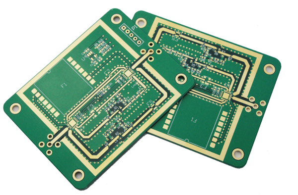
PCB design and PCB and PCBA production and subsequent use have a very close relationship. The outer layer of production and the inner layer of production have many similarities, This article introduces the PCB production of the outer layer and anti-solder station production and PCB design.
Table of Contents
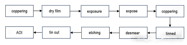
01. outer layer process
(1) a plating to the final copper thickness of the outer layer process, the production process with the inner layer process;
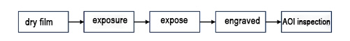
(2) two plating to the final copper thickness of the outer layer process, and copper plating station completed together; choose a full-board plating or two graphic plating process, need to be based on the PCB design features and board factory process arrangements to determine the current graphic plating is more commonly used;
02. Solderproof process
After the outer line is done, the negative will be transformed into the outer line of green oil on the copper foil, revealing the need to weld the PAD and holes.
If there is a need to plug holes, if the holes are to be filled, you can use resin to plug holes, you can also use green oil to plug holes; if the holes do not need to be filled, you can choose to cover the holes with green oil, the small via holes in the green oil printing or showering process will be plugged by the green oil, but generally will not be filled;
03. Copper thickness design
Outer layer copper thickness for PCB layers greater than or equal to 2 of the board, are plated from the bottom copper to the final copper thickness; outer layer copper plating thickness is generally about 1.5 times the thickness of the hole copper, the board factory will adjust the copper-plating parameters to meet the copper thickness of the PCB;
Therefore, PCB designers label the outer layer of copper thickness to indicate the final copper thickness or bottom copper thickness.
The final copper thickness determines the line width and line spacing design value, line width and line spacing and etching the difference between the upper and lower line widths and impedance values also has a certain impact.
Device selection should also be matched with the copper thickness, there are fine foot device PCB, copper thickness is too thick, it will lead to device pin spacing that is too close, making soldering is easy prone to tin bad.
Revision of the PCB if you need to increase the copper thickness, be sure to determine the line spacing and fine foot device spacing is matched with the copper thickness, so as not to cause difficulties in the production of PCBs, soldering leads to tin and other bad.
04. Alignment
Outer alignment design is not reliable board edge too close, exposure etching and molding station will have a tolerance, to meet these tolerances, and then consider the production process and turnover of the collision, to avoid the board edge of the exposed copper and the external force bruises, so close to the board edge of the wire, especially the fine line need to leave more distance;
Outer layer alignment, line width line distance to consider the finished copper thickness and the board factory copper plating process, using the graphic plating process, the line distance can be made smaller, using the whole board plating process, the line distance to stay a little more.
Connected to the table PAD alignment, a device of the two PAD alignment to try to symmetry, to ensure that the two PAD area is the same, to prevent the device over the furnace skewed displacement, etc.; table PAD pieces of smaller alignment try to use a thin line to ensure that the area of the PAD is close to the design value, to avoid welding pins less tin;
05. Surface-mounted parts pad PAD
Table sticker welding PAD if the design in the copper foil, its PAD size, that is the size of the anti-solder window, will be larger than the design of the PAD size;
PCB design when the anti-soldering window is generally designed with the same size as the PAD, but PCB production, because the outer layer of etching, negative production, exposure and other tolerances, the negative will generally be the location of the PAD size of a certain size of compensation, that is, increase the size of some to ensure that the PAD will not be covered with green oil to ensure that the welding;
The size of the independent design of the table sticker PAD, closer to the design of the PAD size, anti-solder green oil, and PAD often have a circle between the exposed substrate;
Therefore, the design tries to ensure that the table sticker device pins each end of the design in a unified way, either all independent or all paved with copper, especially for packaging smaller devices, paved with copper should also be the main copper area, can not be too large a difference;
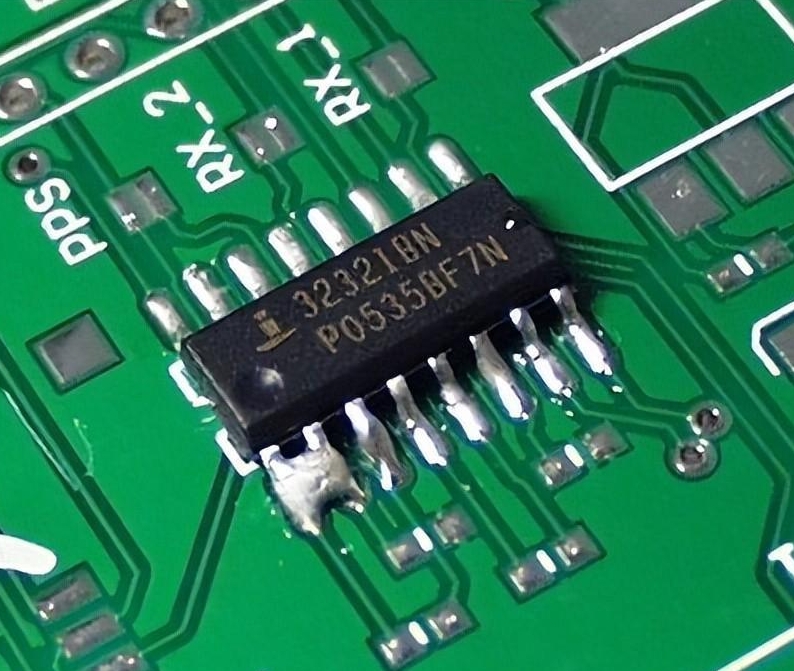
Dense foot device, PAD spacing is small, such as 0.5pitch, anti-soldering compensation on the negative between the two PAD green oil will be very fine or compensation for the two PAD connected; design anti-soldering layer if the device pins for a single window, will cause the green oil bridge can not be made or the green oil bridge falls off; for the fine foot device, you can anti-soldering window open into a whole;
A green oil bridge can reduce the risk of connecting tin to a certain extent, but the control of the amount of solder paste through the stencil can further reduce the risk of connecting tin.
Playing in the heat dissipation PAD over the hole, the hole needs to open the window processing. if the hole is too much, to avoid the solder paste into the hole and affecting the welding, you can design the plug hole. Try not to design the green oil cover hole.
Green oil cover hole hole may be half stuffed with green oil, and the hole around the hole ring part of the green oil, will reduce the overall area of the PAD, affecting heat dissipation, if the solder paste flows into the hole, in addition to lead to less tin, there may be the formation of tin beads and affect the quality of welding;
06. Plug-in soldering PAD
Outer design plug-in soldering PAD, soldering surface PAD if you can lay copper try to lay a small piece of copper, especially for smaller plug-in pins, so as not to weld heat caused by the pad off, laying copper can not be too large, so as not to affect the effect of soldering on the tin;
Some plug-in pin welding PAD will increase some poly heat holes to ensure that the tin, poly heat holes generally need to open the window; welding surface can be PAD and poly heat holes to open the window into a block, and the device surface can be separated from the window.
07. Large copper foil window
To increase the heat dissipation capacity of the large copper foil, the large copper foil will be open window, not covered with green oil, so that the soldering surface in the wave soldering will be on the tin; to better on the tin effect, the soldering surface of the copper foil open window into a line, preferably along the direction of the furnace; over the furnace can increase the amount of solder paste, better heat dissipation;
The window of the device surface can be opened to a large area, the entire copper foil is open;
08. Common defects of the outer layer solder-proof station
Outer station common bad, such as line fine, line jagged, open, short circuit, etching is not net, pad mutilation, excessive etching, etc.; most of them are related to the PCB process, as long as the design process by the ability to design the line width line spacing, PAD laying copper can pay attention to some of the time;
Anti-soldering station common bad, such as green oil on the PAD, exposed copper, green oil bridge off, green oil blistering, green oil into the hole, etc.; therefore, the design should pay attention to the spacing of the smaller PAD window way, the hole of the cover oil way and so on;