Índice
1. Introducción a los PCB y los componentes principales
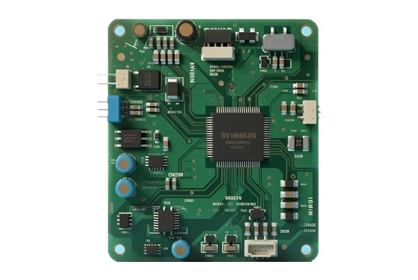
Circuitos impresos (PCB) son componentes fundamentales en la industria electrónica. Sus funciones principales incluyen transmisión de señales, apoyo físico, distribución de energíay gestión térmica. Una PCB comprende varios elementos especializados: el capa serigráfica (Superposición) para la identificación de componentes, acabados superficiales (como ENIG, HASL), vías para conexiones eléctricas entre capas, Componentes de orificio pasante (PTH) y Dispositivos de montaje superficial (SMD), cobro de cobre (Polígono), almohadillas térmicas de alivio, trazas de señales (Pista) y almohadillas, entre otras características fundamentales.
2. Sistema de clasificación de PCB
2.1 Clasificación según el material del sustrato
Sustratos cerámicos: Utilizing materials like Alumina (Al₂O₃), Aluminum Nitride (AlN), or Silicon Carbide (SiC), these offer exceptional thermal conductivity and are designed for high-temperature environments and high-power applications.
PCB con núcleo metálico (MCPCB): Incluyen sustratos a base de aluminio y cobre, conocidos por su excelente disipación del calor, ampliamente utilizados en circuitos de alta potencia e iluminación LED.
Sustratos basados en papel: Como los grados FR-1 y FR-2, utilizan papel de fibra como refuerzo, impregnado con resina y laminado con lámina de cobre, adecuado principalmente para placas de una o dos caras.
Sustratos compuestos: Combinar de forma innovadora las características de múltiples materiales, por ejemplo, CEM-2 (resina epoxi con núcleo de papel y superficies de tela de vidrio), para cumplir requisitos de rendimiento específicos.
2.2 Clasificación según características estructurales
PCB rígidos: Utilice sustratos rígidos no flexibles, incluyendo diversos tipos como FR-4 (epoxi de vidrio), sustratos basados en papel, compuestos, cerámicos y placas con núcleo metálico.
Placas de circuito impreso flexibles (PCB flexibles): emplean sustratos aislantes flexibles, lo que permite doblarlos, enrollarlos y plegarlos, lo que resulta ideal para las limitaciones de espacio de los dispositivos electrónicos portátiles.
Placas de circuito impreso rígido-flexibles: Integra de forma inteligente zonas rígidas y zonas flexibles, ofreciendo tanto resistencia estructural como flexibilidad de instalación.
PCB de IDH (Interconexión de alta densidad): Utiliza tecnología de microvías y láminas de cobre ultradelgadas para satisfacer las exigencias de miniaturización de los dispositivos electrónicos. Las estructuras incluyen vías apiladas en dos pasos, vías escalonadas en dos pasos y HDI en un solo paso.
Sustratos IC: Diseñado específicamente para el encapsulado de chips, proporciona funciones críticas como conexión eléctrica, protección física, soporte estructural y gestión térmica.
3. Análisis en profundidad de la tecnología de sustratos PCB
3.1 Estructura de apilamiento de capas
Las placas de circuito impreso modernas presentan un diseño multicapa:
- Núcleo: Laminado compuesto por tela de fibra de vidrio y resina epoxi, revestido con cobre por ambos lados.
- Preimpregnado (Preimpregnado): compuesto de tela de fibra de vidrio y resina parcialmente curada, responsable de unir las capas durante la laminación.
- Lámina de cobre: Divided into Electro-Deposited (ED) copper (preferred for rigid boards) and Rolled Annealed (RA) copper (used for flexible boards). Thickness is measured in ounces (OZ), e.g., 1 OZ (≈35µm).
3.2 Via Technologies
Las vías de interconexión de PCB se clasifican en tres tipos:
- Viaje a través del agujero: Pasa por todas las capas del circuito.
- Vía ciega: Conecta una capa externa con una o más capas internas, pero no atraviesa toda la placa.
- Enterrado Vía: Situado íntegramente dentro de las capas internas, conectando dos o más capas internas sin llegar a las superficies externas.
3.3 Parámetros clave de rendimiento
Parámetros térmicos:
- Tg (Temperatura de transición vítrea): El punto crítico en el que la resina pasa de un estado rígido a uno más blando, lo que afecta directamente a la resistencia al calor del sustrato.
- Td (Temperatura de descomposición): Temperatura a la que la resina pierde el 5 % de su masa debido a la degradación térmica.
- CTE (Coefficient of Thermal Expansion): Determines dimensional stability under temperature variations. Typically X/Y: 16-18 ppm/°C, Z: 40-60 ppm/°C.
Parámetros eléctricos:
- Dk (Dielectric Constant): Influences signal propagation speed and characteristic impedance. A lower Dk generally allows faster signal speed (V = C/√Dk).
- Df (Factor de disipación): Afecta a la integridad y calidad de la señal; un Df más bajo significa menos pérdida de señal.
- Resistividad superficial/volumétrica: mide el rendimiento conductivo.
Parámetros mecánicos:
- Resistencia a la flexión y resistencia al desprendimiento
- Absorción de agua: afecta a la estabilidad y fiabilidad del sustrato. La humedad puede aumentar el Dk y el riesgo de delaminación («popcorning»).
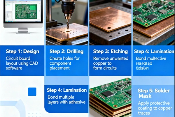
4. Flujo del proceso de fabricación de PCB de precisión
La fabricación de PCB sigue una secuencia estricta:
- Imagen de la capa interna → 2. Laminado fotorresistente → 3. Exposición → 4. Desarrollo → 5. Grabado → 6. Resistencia de tira → 7. Apilamiento de capas → 8. Laminación → 9. Perforación → 10. Recubrimiento (PTH) → 11. Laminado resistente de capa exterior → 12. Exposición → 13. Desarrollo → 14. Recubrimiento de patrones (Cu/Sn) → 15. Resistencia de tira → 16. Grabado → 17. Tira de hojalata → 18. Serigrafía/Impresión de leyendas → 19. Acabado superficial
5. Comparación exhaustiva de los tratamientos de acabado superficial
| Acabado superficial | Características y ventajas principales | Limitaciones / Retos | Nivel de costes | Thickness Range (µm) | Vida útil |
|---|---|---|---|---|---|
| HASL (sin plomo) | Adecuado para almohadillas grandes, espaciado amplio | No es ideal para HDI; alta temperatura; superficie irregular. | Medio-alto | 2-5 (en la almohadilla) | 12 meses |
| HASL (a base de plomo) | Excelente resistencia mecánica | Preocupación medioambiental (contenido en Pb) | Medio-alto | 2-5 (en la almohadilla) | 12 meses |
| OSP | Proceso sencillo, bajo coste. | No apto para múltiples reflujos; inspección difícil. | Más bajo | 0.1 – 0.5 | 6 meses |
| ENIG (Níquel químico/Oro por inmersión) | Soldadura fiable, superficie plana, buena resistencia a la corrosión. | Potencial de «Black Pad» (corrosión del níquel), «Gold Embrittlement» (fragilidad del oro) | Alta | Ni: 3-5 / Au: 0,03-0,08 | 12 meses |
| ENEPIG (Níquel químico/paladio químico/oro por inmersión) | Aplicaciones de alta gama, resistencia superior a la corrosión, apto para soldadura por hilo. | Control complejo del proceso, posibilidad de manchas negras/decoloración. | Alta | Ni: 2-5 / Pd: 0,05-0,15 / Au: 0,05-0,15 | 6 meses |
| Plata de inmersión (ImAg) | Superficie plana, adecuada para múltiples reflujos. | Se empaña fácilmente, requiere condiciones de almacenamiento estrictas. | Medio | 0.1 – 0.5 | 12 meses |
| Lata de inmersión (ImSn) | Buena planitud, soldabilidad | Riesgo de formación de bigotes de estaño, mala resistencia al envejecimiento térmico. | Low | 0.8 – 1.2 | 6 meses |
| Ni/Au electrolítico (Oro suave) | Excelente resistencia al desgaste, fiabilidad de contacto. | Alto consumo de oro, posibles problemas de adhesión de la máscara de soldadura sobre el oro. | Más alto | Ni: 3-5 / Au: ≥0.05 (selective) | 12 meses |
| Oro duro electrolítico | Resistencia extrema al desgaste (por ejemplo, para los dedos). | Mayor coste, proceso más complejo | Más alto | 0,3 – 3,0 (al contacto) | 12 meses |