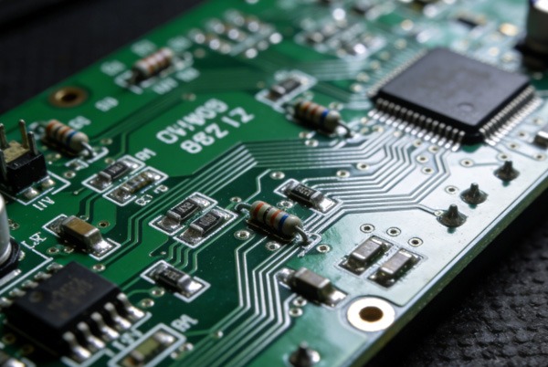
En la era actual de rápida evolución de los productos electrónicos, el diseño de placas de circuito impreso (PCB) ya no se limita únicamente al rendimiento eléctrico, sino que determina directamente la eficiencia de la producción y la fiabilidad del producto final. Orientado a la ensamblaje Diseño de PCB (Diseño para el montaje, DFA) es un enfoque de ingeniería sistemático destinado a optimizar la fabricabilidad de una placa desde el origen, reducir los errores de producción, disminuir los costes y acelerar el tiempo de comercialización.
Este artículo profundizará en los principios básicos, los errores comunes y el valor práctico del diseño del montaje de placas de circuito impreso. Como experto en la fabricación de placas de circuito impreso, TOPFAST ofrece montaje integral de placas de circuito impreso servicios para eliminar sus preocupaciones.
Índice
¿Por qué es fundamental el diseño de PCB orientado al montaje?
1.1 Impacto clave en el proceso de producción
El diseño de PCB no solo influye en la funcionalidad del circuito, sino que también está directamente relacionado con la complejidad del proceso de montaje. Las estadísticas muestran que Los costes determinados durante la fase de diseño representan más del 70 % del coste total de un producto.. Un diseño deficiente puede provocar:
- Retrasos en la producción: Reparación causada por una colocación inadecuada de los componentes o problemas de soldadura.
- Aumento de los costes: Aumento de las repeticiones, los índices de desechos y los problemas de compatibilidad de los equipos.
- Riesgos de fiabilidad: Fallos tempranos provocados por una gestión térmica deficiente o por estrés mecánico.
1.2 Valor fundamental del diseño para el montaje (DFA)
Al implementar los principios de DFA, las empresas pueden:
- Mejorar la compatibilidad de la automatización: Adaptarse a equipos de producción modernos, como máquinas de colocación y hornos de reflujo.
- Optimizar la gestión térmica: Evite daños térmicos durante la soldadura y el funcionamiento.
- Reducir los errores humanos: Minimizar los errores de funcionamiento durante el montaje mediante un diseño estandarizado.
Seis principios fundamentales de Montaje de PCB Diseño
2.1 Optimización de la colocación de componentes
- Agrupación de componentes similares y orientación uniforme: Concentrar componentes similares, como resistencias y condensadores, y mantener una orientación uniforme (por ejemplo, todos los componentes polares orientados hacia el norte) puede Mejorar la eficiencia de las máquinas de recogida y colocación hasta en un 20 %..
- Control racional del espaciado:
- Small component spacing ≥ 0.5mm.
- Large component spacing ≥ 1–2mm.
- Components should be ≥ 3mm from the board edge to avoid assembly interference.
- Aislamiento de componentes sensibles al calorMantenga los componentes que generan mucho calor (por ejemplo, transistores de potencia) alejados de dispositivos sensibles como microcontroladores para evitar daños térmicos durante la soldadura o el funcionamiento.
2.2 Adaptación del proceso de soldadura
- Diseño de almohadillas SMT:
- Toe Extension: 0.2–0.5mm, promotes solder flow.
- Heel Extension: 0.1–0.3mm, enhances solder joint strength.
- Puede mejorar la fiabilidad de las juntas soldadas mediante más del 15 %.
- Tamaño de la almohadilla del componente de orificio pasante: Pad diameter should be 1.5–2 times the lead diameter.
- Gestión del estrés térmicoEvite colocar capas gruesas de cobre directamente debajo de componentes pequeños; considere añadir almohadillas térmicas de 0,25 mm para equilibrar la distribución del calor.
- Adaptación del proceso de soldadura:
- Soldadura por ola: Coloque los componentes SMT sensibles en el lado opuesto de la placa.
- Reflow Soldering: Ensure all components can withstand peak temperatures (typically ~260°C for lead-free solder).
2.3 Normalización y gestión de bibliotecas
- Adopte las huellas estándar IPC (por ejemplo, IPC-7351), lo que reduce los errores de colocación en un 10%.
- Marcado claro de polaridad: Marque explícitamente la polaridad de los diodos y condensadores electrolíticos en la capa de serigrafía.
- Verificación de componentes de bibliotecaAsegúrese de que las huellas coincidan con las dimensiones físicas de los componentes para evitar errores en el paso de los pines.
2.4 Optimización para el montaje automatizado
- Diseño de panelización: Connect multiple boards via V-scoring or tab-routing, leaving a ≥ 5mm process border.
- Configuración del marcador fiducial:
- Cantidad: al menos 3, colocadas cerca de las esquinas del tablero.
- Tamaño: 1 mm de diámetro, con un espacio libre (sin cobre) de 3 mm alrededor de cada uno.
- Optimización de la orientación de los componentes: Minimizar la rotación del cabezal de recogida y colocación, lo que podría aumentar la velocidad en 5–10%.
2.5 Limitaciones del proceso de fabricación
- Relación de aspecto del taladro: Maintain between 10:1 and 20:1 (e.g., for a 1.6mm board, minimum via diameter should be ≥ 0.08mm).
- Ancho de traza/espacio: Mínimo 0,1 mm para procesos estándar.
- Espesor estándar de la placa: Prefiera espesores comunes como 1,6 mm, 0,8 mm.
2.6 Integridad de la documentación
- Lista de materiales: Incluya los números de pieza, las cantidades y los números de pieza alternativos.
- Planos de montaje: Indique claramente la ubicación de los componentes, su orientación y cualquier nota especial sobre el proceso.
- Archivos Gerber: Coloque y etiquete correctamente las capas de cobre, máscara de soldadura y serigrafía.
3. Errores comunes en el diseño del montaje de placas de circuito impreso y estrategias para evitarlos
| Error común | Impacto potencial | Estrategia de evitación |
|---|---|---|
| Espaciado insuficiente entre componentes | Solder bridges, mechanical interference; defect rate increase of 15–20% | Cumpla con las normas de espaciado IPC y deje espacio para el alivio térmico. |
| Falta de gestión térmica | Daños en los componentes durante la soldadura o el funcionamiento. | Añada vías térmicas o almohadillas disipadoras de calor para los componentes de alta potencia. |
| Marcas poco claras en la serigrafía | Componentes de polaridad inversa que provocan fallos en el circuito. | Utilice símbolos estandarizados y asegúrese de que las marcas sean legibles. |
| Uso de huellas no estándar | Incompatibilidad de equipos, paradas de producción | Cumpla con las normas IPC y verifique previamente los componentes de la biblioteca. |
4. Ventajas fundamentales del diseño orientado al ensamblaje
- Reducción de costes: El diseño optimizado reduce la necesidad de reelaboraciones, lo que puede suponer un ahorro de hasta 30% en los costes de producción.
- Reducción del tiempo de ciclo: La compatibilidad mejorada con la automatización acelera el flujo de producción, reduciendo el tiempo de entrega en 10–15%.
- Fiabilidad mejorada: Un diseño adecuado de la soldadura y la gestión térmica reduce significativamente las tasas de fallos en el campo.
- Escalabilidad mejoradaEl diseño estandarizado facilita la iteración del producto y la producción en masa.
5. Conclusión
El diseño de PCB orientado al montaje es el puente fundamental que conecta el diseño eléctrico con la fabricación en serie. Por aplicar sistemáticamente los principios del DFA—from component placement and soldering optimisation to standardised library management, automation adaptation, and manufacturing constraint consideration—companies can establish efficient, reliable, and economical product production processes.
En el contexto de la rápida evolución del hardware inteligente y la competencia cada vez más feroz en el mercado, Incorporar la capacidad de fabricación en el ADN del diseño. se ha convertido en una competencia fundamental para los ingenieros. Ya sea para la creación de prototipos o la producción en masa, seguir estas directrices no solo ayuda a evitar errores comunes, sino que también sienta una base sólida para la alta fiabilidad del producto, la rapidez de comercialización y el control de costes.
El diseño determina la fabricación, los detalles determinan el éxito. En su próximo proyecto, intente integrar estos principios en su flujo de trabajo de diseño y observe cómo su PCB pasa de ser un proyecto a convertirse en un producto estable y fiable.

Problemas comunes y soluciones profesionales
A:Manifestaciones: Puentes de soldadura, tombstoning de componentes, dificultades de soldadura.
Causas: Espaciado insuficiente, diseño térmico desequilibrado.
Soluciones:
Maintain component spacing: ≥0.5mm for small components, ≥2mm for large components
Mantenga los componentes que generan calor alejados de los dispositivos sensibles a la temperatura.
Dimensiones de la almohadilla de diseño según las normas IPC.
A: Manifestaciones: La fábrica no puede procesar, alta tasa de rechazo del primer artículo.
Causas: Supervisar las capacidades de fabricación de la fábrica.
Soluciones:
Confirme el ancho/espaciado mínimo de traza de fábrica antes del diseño (normalmente 0,1 mm).
Utilice tableros de grosor estándar (el más habitual es 1,6 mm).
Ensure that the dimensions comply with the aspect ratio ≤8:1
A: Manifestaciones: Sobrecalentamiento de los componentes, reducción de la vida útil.
Causas: Fuentes de calor concentradas, vías de disipación del calor deficientes.
Soluciones:
Distribuir los componentes generadores de calor por toda la placa.
Añadir matrices de vías térmicas
Reserve 100mm² copper area per watt of power
A: Manifestaciones: Se han utilizado componentes incorrectos, errores de montaje.
Causas: Lista de materiales poco clara, falta información en los planos.
Soluciones:
Especifique piezas alternativas y parámetros clave en la lista de materiales.
Marque todos los indicadores de polaridad en los planos de montaje.
Asegúrese de que los archivos Gerber contengan capas completas.
A: Manifestaciones: Cobertura de pruebas inadecuada, reparaciones difíciles.
Causas: No hay puntos de prueba reservados, espacio insuficiente para reparaciones.
Soluciones:
Incluir puntos de prueba para todas las redes críticas.
Test point diameter ≥1mm, spaced at 2.54mm intervals
Reservar posiciones para interfaces de depuración estándar.