Table des matières
1. Principaux avantages du cuivre en tant que matériau préféré pour les circuits imprimés
1.1 Des performances électriques inégalées
- Second only to silver in conductivity, the resistivity of 1.68 × 10⁻⁸ Ω·m ensures efficient signal transmission.
- Excellente réponse aux hautes fréquences: Maintient des caractéristiques d'impédance stables malgré les effets de la peau.
- Capacité supérieure de transport de courant: Capacité de courant supérieure de 40 % à celle de l'aluminium pour une même surface de section.
1.2 Compatibilité exceptionnelle des processus
- Capacité de gravure de précision: Prise en charge des traces ultrafines inférieures à 3 mil.
- Pelliculage multicouche: Correspond au coefficient d’expansion thermique (CTE) du FR4.
- Finitions de surface polyvalentes: Compatible avec tous les procédés courants (ENIG/OSP/HASL).
1.3 Analyse coût-efficacité
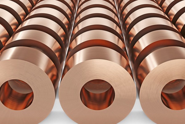
- Coût des matériaux: Prix de 1/50e de l'argent et seulement 1,2x de l'aluminium.
- Coût de la transformation: Les processus matures permettent d'obtenir des taux de réussite de la production supérieurs à 98 %.
- Recyclabilité: Taux de récupération du cuivre de plus de 95 % à partir de panneaux de ferraille.
2. Valeur technique des techniques de coulée du cuivre
2.1 Compatibilité électromagnétique (CEM) améliorée
- Efficacité du blindage: La coulée de cuivre intégrale réduit les interférences rayonnées de >15dB.
- Chemins de retour du signal: Fournit les chemins de retour les plus courts pour les signaux à grande vitesse.
- Contrôle de l'impédanceMaintient des caractéristiques cohérentes de la ligne de transmission.
2.2 Amélioration de la gestion thermique
- Conductivité thermique: Outstanding 398W/(m·K) heat dissipation capability.
- Conception de la diffusion de la chaleur: Prévient les points chauds localisés.
- Refroidissement du dispositif d'alimentation: Epaisseur de cuivre en fonction de la référence de capacité de courant :
| Épaisseur de cuivre (oz) | Largeur de la trace (mm) par 1A |
|---|---|
| 1 | 0.4 |
| 2 | 0.2 |
| 3 | 0.13 |
2.3 Optimisation de la résistance mécanique
- Résistance à la flexion: Augmente la rigidité du substrat de >30%.
- Stabilité dimensionnelle: Résiste à la déformation due aux changements de température et d'humidité.
- Résistance aux vibrations: Obligatoire pour les applications militaires.
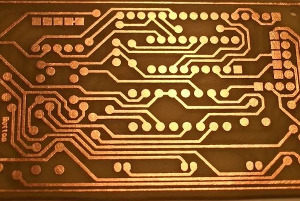
3. Guide pratique de la conception des coulées de cuivre
3.1 Comparaison de deux méthodes fondamentales de coulée
Coulée en cuivre massif
- Applications : Plans d'alimentation, circuits à courant élevé
- Special treatment: Requires thermal relief slots (width ≥0.5mm)
- Paramètres typiques :1-3oz d'épaisseur, <30% de taux d'ouverture
Grille Coulée de cuivre
- Meilleures utilisations : Zones de signaux à haute fréquence
- Grid specifications: Line width/spacing ≥5mil
- Avantages :Réduction des contraintes thermiques, réduction du poids de 15
3.2 Normes de traitement des zones spéciales
- Zones d'antennes: Maintenir un espace de 20 mm
- Sous BGA: Utiliser des connexions de tampons en forme de croix
- Bords du panneau: Implement ≥3mm copper rings
3.3 Erreurs de conception courantes et corrections
- Îles du cuivre: Éliminer les vias de mise à la terre
- Angles vifs: Replace with curved transitions (radius ≥3x trace width)
- Dissipation inégale de la chaleur: Mise en œuvre de gradients progressifs d'épaisseur de cuivre
- Désadaptation de l'impédance: Contrôle strict des tolérances d'épaisseur de la couche diélectrique
- Défauts de soudure: Optimiser les dimensions de l'ouverture du masque de soudure
4. Évolution des frontières de l'industrie
- Feuilles de cuivre ultra-minces: Performance in 5G mmWave circuits (12μm thickness)
- Solutions de matériaux hybrides: Données d'essais thermiques pour les composites cuivre-graphène
- Circuits en cuivre imprimés en 3D: Percées de précision dans la technologie LDS
- Traitement respectueux de l'environnement: Progrès dans la métallisation du cuivre sans cyanure