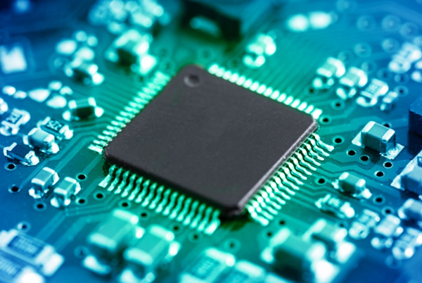
Dans le domaine de la conception électronique, le choix du bon nombre de couches de PCB est l'un des facteurs clés de la réussite d'un projet. En tant qu'équipe technique ayant 17 ans d'expérience dans la fabrication de circuits imprimés, TopFast vous propose d'explorer en profondeur les principales différences entre les circuits imprimés monocouches et les circuits imprimés bicouches.
Table des matières
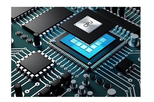
Concepts de base des PCB
Qu'est-ce qu'un circuit imprimé monocouche ?
Le circuit imprimé à couche unique est le type de circuit imprimé le plus élémentaire :
- 1 conductive copper foil layer (typically 35μm thick)
- 1 substrat FR-4 couche de matériau
- Couche de sérigraphie simple face
- Couche de masque de soudure simple face
Les scénarios d'application typiques sont les suivants
- Tableaux de commande d'appareils simples (par exemple, minuteries de ventilateurs)
- Pilotes d'éclairage LED
- Circuits électroniques de contrôle des jouets
Qu'est-ce qu'un circuit imprimé double couche ?
Le circuit imprimé à double couche est une structure de circuit imprimé plus avancée qui contient :
- Couches de cuivre conducteur double face
- Connexions entre les couches par des trous de passage plaqués
- Masque de soudure double face et sérigraphie
- Traitements de surface optionnels (par exemple, HASL, ENIG)
Principaux domaines d'application :
✓ Smart home controllers
✓ Industrial sensor modules
✓ Automotive electronic units
✓ Consumer electronics products
Conseil de pro: Contactez dès maintenant les ingénieurs de TopFast pour obtenir des conseils gratuits sur le choix de la couche. pour obtenir la meilleure solution coût-performance pour votre projet !
Principales différences de performance
1. Différences de performances électriques
| Paramètres | PCB monocouche | PCB double couche |
|---|---|---|
| Fréquence maximale de fonctionnement | 10MHz | 100MHz |
| Intégrité du signal | Pauvre | Excellent |
| Capacité anti-interférence | Faible | Fort |
| Bruit de l'alimentation | Haut | Low |
2.Comparaison de la flexibilité de la conception
Les circuits imprimés à double couche offrent des options de conception plus souples :
- La technologie de mise à la terre du réseau est disponible
- Prise en charge de la segmentation du plan d'alimentation
- Permet de mieux placer les composants
- Permet de raccourcir les chemins de retour des signaux
3.Analyse des coûts de fabrication
Bien que les circuits imprimés à double couche aient des coûts initiaux plus élevés, il convient de les prendre en considération :
- Réduction de la surface de la carte (gain de place de 20 à 40 %)
- Réduction des coûts de modification ultérieure
- Amélioration de la fiabilité des produits
Le coût total réel peut être inférieur
Solution d'optimisation des coûts: Obtenez le plan exclusif d’optimisation des coûts des circuits imprimés double couche de TopFastavec des économies potentielles allant jusqu'à 30 % des coûts de production !
Sélection de cartes simple face et double face
Quand choisir un circuit imprimé monocouche ?
✓ Extremely limited budget prototyping stage
✓ Simple circuits with operating frequency <1MHz
✓ Products without strict size requirements
✓ Applications not requiring impedance control
Quand faut-il choisir un circuit imprimé double couche ?
➤ Digital circuits with operating frequency >10MHz
➤ Scenarios requiring strict impedance control
➤ High-density component layout requirements
➤ Applications with EMC/EMI requirements
Avantages de la fabrication professionnelle de TopFast
Nous fournissons des solutions professionnelles pour tous les types de besoins en matière de PCB :
Points forts du service PCB monocouche :
- Prototypage rapide en 24 heures
- Starting at just $0.1/board (approx. ¥0.7)
- Epaisseur standard de 1,6 mm
- Masque de soudure vert standard avec sérigraphie blanche
Capacités techniques en matière de circuits imprimés double couche :
✔ 6mil (0.15mm) precision trace width/spacing
✔ 0.2mm minimum via size
✔ Multiple surface treatment options
✔ 100% flying probe testing
Planifiez dès maintenant une consultation avec le conseiller technique de TopFast pour obtenir des solutions PCB personnalisées !