Table des matières
1. Introduction aux circuits imprimés et aux composants essentiels
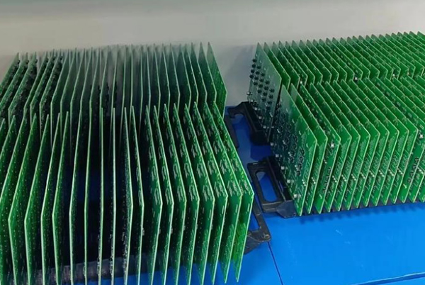
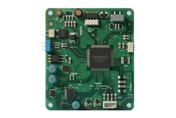
Cartes de circuits imprimés Les circuits imprimés (PCB) sont des composants fondamentaux dans l'industrie électronique. Leurs principales fonctions sont les suivantes : transmission du signal, soutien physique, distribution de puissanceet gestion thermique. Un circuit imprimé comprend divers éléments spécialisés : le couche sérigraphiée (Superposition) pour l'identification des composants, finitions de surface (telles que ENIG, HASL), vias pour les connexions électriques intercouches, Composants à trous traversants (PTH) et Dispositifs à montage en surface (SMD), coulées de cuivre (Polygone), coussins thermiques, traces de signaux (Piste), et tampons, entre autres fonctionnalités essentielles.
2. Système de classification des PCB
2.1 Classification selon le matériau du substrat
Substrats céramiques: Utilizing materials like Alumina (Al₂O₃), Aluminum Nitride (AlN), or Silicon Carbide (SiC), these offer exceptional thermal conductivity and are designed for high-temperature environments and high-power applications.
Circuits imprimés à noyau métallique (MCPCB) : comprenant des substrats à base d'aluminium et de cuivre, connus pour leur dissipation thermique supérieure, largement utilisés dans les circuits haute puissance et l'éclairage LED.
Supports papier: Telles que les qualités FR-1 et FR-2, utilisent du papier fibreux comme renfort, imprégné de résine et laminé avec une feuille de cuivre, principalement adapté aux cartes simple ou double face.
Substrats composites: Combiner de manière innovante les caractéristiques de plusieurs matériaux, par exemple le CEM-2 (résine époxy avec un noyau en papier et des surfaces en tissu de verre), afin de répondre à des exigences de performance spécifiques.
2.2 Classification selon les caractéristiques structurelles
PCB rigides: Utilisez des substrats rigides non flexibles, notamment divers types tels que FR-4 (verre époxy), à base de papier, composites, céramiques et à âme métallique.
Circuits imprimés souples (Circuits imprimés flexibles) : utilisent des substrats isolants flexibles, pouvant être pliés, enroulés et repliés, ce qui les rend idéaux pour les appareils électroniques portables soumis à des contraintes d'espace.
Circuits imprimés rigides et flexibles: Intégrer intelligemment des zones rigides et des zones flexibles, offrant à la fois une résistance structurelle et une flexibilité d'installation.
Cartes de circuits imprimés HDI (Interconnexion haute densité) : utilise la technologie des microvias et des feuilles de cuivre ultrafines pour répondre aux exigences de miniaturisation des appareils électroniques. Les structures comprennent des vias empilés en deux étapes, des vias décalés en deux étapes et des HDI en une étape.
Substrats IC: Conçu spécialement pour l'emballage des puces, il assure des fonctions essentielles telles que la connexion électrique, la protection physique, le soutien structurel et la gestion thermique.
3. Analyse approfondie de la technologie des substrats PCB
3.1 Structure d'empilement des couches
Les circuits imprimés modernes présentent une conception multicouche :
- Noyau: Stratifié composé d'un tissu en fibre de verre et de résine époxy, recouvert de cuivre sur les deux faces.
- Préimprégné (Préimprégné) : Composite constitué d'un tissu en fibre de verre et d'une résine partiellement durcie, qui sert à coller les couches entre elles pendant le laminage.
- Feuille de cuivre: Divided into Electro-Deposited (ED) copper (preferred for rigid boards) and Rolled Annealed (RA) copper (used for flexible boards). Thickness is measured in ounces (OZ), e.g., 1 OZ (≈35µm).
3.2 Via Technologies
Les vias d'interconnexion des circuits imprimés sont classés en trois types :
- Via traversant: Traverse toutes les couches du circuit.
- Via aveugle: Relie une couche externe à une ou plusieurs couches internes, mais ne traverse pas toute la carte.
- Enterré Via: Situé entièrement dans les couches internes, reliant deux ou plusieurs couches internes sans atteindre les surfaces externes.
3.3 Paramètres clés de performance
Paramètres thermiques:
- Tg (Température de transition vitreuse) : Point critique où la résine passe d'un état rigide à un état plus souple, ce qui a un impact direct sur la résistance thermique du substrat.
- Td (Température de décomposition) : Température à laquelle la résine perd 5 % de sa masse en raison de la dégradation thermique.
- CTE (Coefficient of Thermal Expansion): Determines dimensional stability under temperature variations. Typically X/Y: 16-18 ppm/°C, Z: 40-60 ppm/°C.
Paramètres électriques:
- Dk (Dielectric Constant): Influences signal propagation speed and characteristic impedance. A lower Dk generally allows faster signal speed (V = C/√Dk).
- Df (Facteur de dissipation) : affecte l'intégrité et la qualité du signal ; un Df plus faible signifie moins de perte de signal.
- Résistivité superficielle/volumique : mesure la conductivité.
Paramètres mécaniques:
- Résistance à la flexion et résistance au pelage
- Absorption d'eau : influe sur la stabilité et la fiabilité du substrat. L'humidité peut augmenter le Dk et le risque de délamination (« popcorning »).
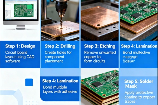
4. Processus de fabrication de circuits imprimés de précision
La fabrication des circuits imprimés suit une séquence rigoureuse :
- Imagerie de la couche interne → 2. Laminage de photoréserve → 3. Exposition → 4. Développement → 5. Gravure → 6. Bande résistante → 7. Empilement de couches → 8. Lamination → 9. Forage → 10. Placage (PTH) → 11. Laminage résistant à la couche externe → 12. Exposition → 13. Développement → 14. Placage de motifs (Cu/Sn) → 15. Bande résistante → 16. Gravure → 17. Bande de fer-blanc → 18. Sérigraphie/Impression de légendes → 19. Finition de la surface
5. Comparaison complète des traitements de finition de surface
| Finition de la surface | Caractéristiques et avantages clés | Limites / Défis | Niveau de coût | Thickness Range (µm) | Durée de conservation |
|---|---|---|---|---|---|
| HASL (sans plomb) | Convient aux coussinets de grande taille, espacement large | Non idéal pour l'IDH ; température élevée ; surface inégale | Moyen-élevé | 2-5 (sur bloc-notes) | 12 mois |
| HASL (à base de plomb) | Excellente résistance mécanique | Préoccupation environnementale (teneur en Pb) | Moyen-élevé | 2-5 (sur bloc-notes) | 12 mois |
| OSP | Processus simple, faible coût | Ne convient pas à plusieurs refusions ; inspection difficile | Le plus bas | 0.1 – 0.5 | 6 mois |
| ENIG (Ni chimique/Au par immersion) | Soudure fiable, surface plane, bonne résistance à la corrosion | Risque de « Black Pad » (corrosion du nickel) et de « Gold Embrittlement » (fragilisation de l'or) | Haut | Ni : 3-5 / Au : 0,03-0,08 | 12 mois |
| ENEPIG (Ni/Pd/Au par immersion sans courant) | Applications haut de gamme, résistance supérieure à la corrosion, soudable par fil | Contrôle complexe du processus, risque de taches noires/décoloration | Haut | Ni : 2-5 / Pd : 0,05-0,15 / Au : 0,05-0,15 | 6 mois |
| Argent par immersion (ImAg) | Surface plane, adaptée à plusieurs refusions | Se ternit facilement, nécessite des conditions de stockage strictes | Moyen | 0.1 – 0.5 | 12 mois |
| Étain d'immersion (ImSn) | Bonne planéité, soudabilité | Risque de formation de whiskers d'étain, mauvaise résistance au vieillissement thermique | Low | 0.8 – 1.2 | 6 mois |
| Ni/Au électrolytique (Or tendre) | Excellente résistance à l'usure, fiabilité de contact | Consommation élevée d'or, problèmes potentiels d'adhérence du masque de soudure sur l'or | Le plus élevé | Ni: 3-5 / Au: ≥0.05 (selective) | 12 mois |
| Or dur électrolytique | Résistance extrême à l'usure (par exemple, pour les doigts) | Coût le plus élevé, processus le plus complexe | Le plus élevé | 0,3 – 3,0 (au contact) | 12 mois |