
Cartes de circuits imprimés Les circuits imprimés (PCB) sont les piliers fondamentaux des appareils électroniques modernes. À mesure que les appareils tendent vers des fréquences plus élevées, des vitesses plus rapides et une miniaturisation croissante, une conception optimale de la disposition des PCB est devenue un facteur déterminant pour les performances des produits. Cet article explore les techniques avancées de disposition des PCB, telles que le routage à haute vitesse, le contrôle de l'impédance et l'optimisation de l'intégrité de l'alimentation, afin d'aider les ingénieurs à concevoir des cartes de circuits imprimés plus fiables et plus efficaces.
Table des matières
Technologie de routage à haut débit
Principe de la trace courte et droite
Le routage des signaux à haute vitesse doit suivre la principe du shoCheminement optimal, minimisant les courbes et les virages inutiles. Le maintien d'une géométrie de trace cohérente réduit considérablement le risque de retard et de distorsion du signal.
Points clés de mise en œuvre :
- Donnez la priorité au routage des chemins de signaux critiques à haute vitesse.
- Évitez les angles à 90 degrés ; utilisez plutôt des angles à 45 degrés ou des virages en arc.
- Maintenir une largeur et un espacement uniformes des traces.
Stratégie de routage des paires différentielles
Le routage différentiel des signaux est une méthode efficace pour lutter contre Interférences électromagnétiques (EMI) et diaphonie :
| Avantage | Méthode de mise en œuvre |
|---|---|
| Forte réjection du bruit en mode commun | Maintenir une correspondance stricte des longueurs pour les paires différentielles. |
| Réduction du rayonnement EMI | Contrôlez l'espacement constant au sein de la paire différentielle. |
| Intégrité du signal améliorée | Évitez les divisions dans les plans de référence sous les paires différentielles. |
Optimisation de la disposition des composants
Le placement stratégique des composants peut réduire considérablement la surface de la boucle de signal :
- Disposition des cloisons selon les modules fonctionnels.
- Réduire les distances d'interconnexion entre les appareils à haut débit.
- Évitez la proximité entre les lignes de signaux sensibles et les sources de bruit.
Technologie de contrôle d'impédance
Relation entre la largeur de piste et l'impédance
Obtenir l'impédance caractéristique cible grâce à un calcul et un ajustement précis de la largeur des pistes :
Stratégies courantes de contrôle d'impédance :
- Use outils de calcul d'impédance pour une simulation précise.
- Tenir compte de la structure empilée du circuit imprimé et des propriétés du matériau diélectrique.
- Définissez les cibles d'impédance correspondantes pour différents types de signaux.
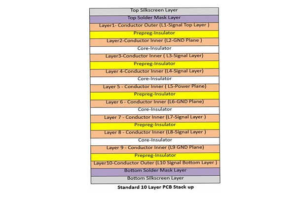
Optimisation de la conception par empilement
Une conception rationnelle par empilement garantit une impédance constante sur l'ensemble de la carte :
Recommandé Empilement à 4 couches Structure :
Couche supérieure : couche de signal (structure microbande)
Couche 2 : plan de masse
Couche 3 : plan d'alimentation
Couche inférieure : couche de signal (structure à ligne triplaque)
Sélection des matériaux diélectriques
Sélectionner matériaux diélectriques stables est crucial pour le contrôle de l'impédance :
- Faites attention à la constante diélectrique (Dk) et au facteur de dissipation (Df) du matériau.
- Tenez compte de la stabilité de la température et des caractéristiques de fréquence.
- Privilégiez les matériaux à faibles pertes pour les applications à haute fréquence.
Optimisation de l'intégrité de l'alimentation électrique
Stratégie de disposition des condensateurs de découplage
Les condensateurs de découplage constituent la première ligne de défense pour maintenir la stabilité de l'alimentation électrique :
Programme de découplage progressif :
- Bulk Capacitors (10-100μF): Placé aux points d'entrée d'alimentation pour gérer les fluctuations à basse fréquence.
- Medium Capacitors (0.1-1μF): Réparti sur toute la bande pour couvrir la gamme des fréquences moyennes.
- Small Capacitors (0.01-0.1μF): Placé à proximité des broches d'alimentation de l'appareil afin de supprimer les bruits à haute fréquence.
Réseau de distribution d'énergie à faible impédance (PDN)
Méthodes pour construire un PDN à faible impédance :
- Utilisez des plans d'alimentation et de masse solides.
- Utilisez judicieusement les vias pour connecter l'alimentation entre les différentes couches.
- Réduisez l'inductance série dans le circuit d'alimentation.
Simulation de l'intégrité de l'alimentation électrique
Utilisez des outils tels que SPICE and HyperLynx pour la simulation précoce :
- Identifier les problèmes potentiels liés au bruit électrique.
- Optimisez la quantité et l'emplacement des condensateurs de découplage.
- Vérifiez la chute de tension et la marge de bruit.
Méthodes d'atténuation des interférences électromagnétiques/compatibilité électromagnétique
Optimisation des techniques de mise à la terre
Une mise à la terre adéquate est la base de la conception CEM :
Points clés de la conception de la mise à la terre :
- Utilisez des plans de masse continus et solides.
- Fournir le chemin de retour le plus court pour les signaux à haute fréquence.
- Évitez les fissures et les interstices dans le plan de masse.
Techniques de blindage et de filtrage
Utilisez une combinaison de méthodes pour supprimer les interférences électromagnétiques :
| Type de technique | Scénario d'application | Méthode de mise en œuvre |
|---|---|---|
| Blindage | Protection des circuits sensibles | Écrans métalliques, revêtements conducteurs |
| Filtrage | Suppression des interférences conduites | Filtres EMI, perles de ferrite |
| Résiliation | Réduire les reflets | Résistances d'adaptation source/sortie |
Stratégies de gestion thermique
Conception et disposition des dissipateurs thermiques
- Sélectionnez des dissipateurs thermiques de taille appropriée en fonction de la dissipation de puissance.
- Assurez-vous que le dissipateur thermique est bien en contact avec la surface de la puce.
- Envisagez d'aligner l'orientation du dissipateur thermique avec la direction du flux d'air.
Vias thermiques et coussinets thermiques
- Disposer des réseaux de vias thermiques sous les composants générateurs de chaleur.
- Use thermal pads to increase the散热 area.
- Conduire efficacement la chaleur vers les plans de masse internes.
Gestion du flux d'air
- Tenez compte des chemins d'écoulement de l'air lors du placement des composants.
- Placez les composants à haute température en amont du flux d'air.
- Évitez les composants hauts qui bloquent les voies d'écoulement de l'air.
Principes de conception pour la fabricabilité (DFM)
Points clés du DFM
La mise en œuvre des principes DFM peut améliorer considérablement l'efficacité et le rendement de la production :
Éléments critiques à vérifier pour la DFM :
- La largeur minimale des traces/l'espace libre est conforme aux capacités du fabricant.
- Dimensions et emplacements optimisés des trous de forage.
- Conception standardisée du masque de soudure et de la sérigraphie.
- Prise en compte de la conception des bords de la carte et de la panélisation.
Utilisation d'outils DFM avancés
- Utilisez des outils tels que PCBCart DFM instantané pour la vérification préalable à la conception.
- Obtenez des commentaires en temps réel sur la fabricabilité.
- Identifiez et corrigez rapidement les problèmes potentiels.
Considérations particulières pour la conception de circuits imprimés à signaux mixtes
Partitionnement analogique et numérique
Gérer correctement la relation entre les circuits analogiques et numériques :
Principes de disposition des partitions :
- Séparer physiquement les zones des circuits analogiques et numériques.
- Utilisez des plans d'alimentation et de masse indépendants.
- Mettre en place une mise à la terre en un seul point au niveau des dispositifs ADC/DAC.
Stratégies de mise à la terre des signaux mixtes
Choisissez le schéma de mise à la terre approprié en fonction de la complexité du système :
Schéma à plan de masse unique (Convient aux systèmes à faible courant numérique) :
- Utilisez un seul plan de masse continu.
- Permettre aux courants de retour analogiques et numériques de se séparer naturellement.
Schéma de plan de masse divisé (Convient aux systèmes à courant numérique élevé) :
- Séparer les masses analogiques et numériques.
- Connectez-vous à un seul point près de l'alimentation électrique (mise à la terre en étoile).
- Fournir des chemins de mise à la terre clairs pour les dispositifs à signaux mixtes.
Liste de contrôle pour la disposition des circuits imprimés
Utilisez la liste de contrôle suivante pour effectuer une vérification finale après avoir terminé la mise en page :
- Contrôle de l'intégrité du signal (chemins de signaux à haute vitesse, terminaison, impédance)
- Vérification de l'intégrité de l'alimentation (découplage, impédance PDN)
- Évaluation de la gestion thermique (dissipation thermique pour les composants haute puissance, flux d'air)
- Considérations relatives à la compatibilité électromagnétique (blindage, filtrage, mise à la terre)
- Vérification DFM (limites du processus, tolérances)
- Faisabilité de l'assemblage (espacement des composants, exigences en matière de soudure)
- Accès aux tests et aux retouches (points de test, accès aux sondes)
Conclusion
La maîtrise des techniques avancées de conception de circuits imprimés est essentielle pour concevoir des appareils électroniques hautement performants et fiables. En mettant en œuvre les stratégies de routage à haute vitesse, de contrôle d'impédance, d'optimisation de l'intégrité de l'alimentation et de gestion thermique présentées dans cet article, les ingénieurs peuvent améliorer considérablement les performances des produits tout en réduisant les coûts de production et en améliorant le rendement. À mesure que les appareils électroniques évoluent vers des fréquences plus élevées et des tailles plus petites, ces techniques de conception avancées deviendront de plus en plus importantes.