Os defeitos de fabricação de placas de circuito impresso podem afetar significativamente a confiabilidade do produto, o desempenho elétrico e o rendimento geral da fabricação.
Mesmo pequenos defeitos introduzidos durante a fabricação podem levar a falhas funcionais durante a montagem ou operação em campo.
Neste artigo, TOPFAST, a professional PCB manufacturer, explains the most common PCB manufacturing defects, why they occur, and—most importantly—how to prevent them through proper design and manufacturing control.
Índice
O que são defeitos de fabricação de PCB?
Os defeitos de fabricação de PCB são falhas físicas ou elétricas não intencionais introduzidas durante o processo de fabricação.
Esses defeitos podem ocorrer devido a limitações de projeto, problemas com materiais, instabilidade do processo ou controle de qualidade insuficiente.
Ao contrário dos problemas relacionados com a montagem, os defeitos de fabricação existem no apenas PCB antes de qualquer componente ser montado.
Por que ocorrem defeitos na fabricação de placas de circuito impresso
A maioria dos defeitos em placas de circuito impresso é causada por um ou mais dos seguintes fatores:
- Inadequado DFM Revisão do projeto para fabricação
- Tolerâncias de projeto rigorosas além da capacidade do processo
- Inconsistências materiais
- Variação do processo durante a gravação, laminação ou galvanização
- Inspeção ou testes insuficientes
Compreensão qual etapa de fabricação introduz qual defeito é a chave para a prevenção.
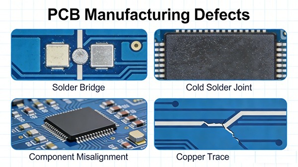
Defeitos mais comuns na fabricação de placas de circuito impresso
Abaixo estão os defeitos de fabricação de PCB mais frequentemente encontrados em ambientes de produção reais.
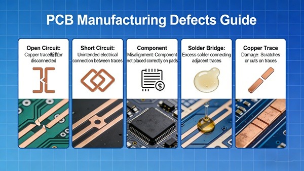
Circuitos abertos
Descrição:
Uma ruptura em um traço de cobre que interrompe a continuidade elétrica.
Causas comuns:
- Gravura excessiva durante o processamento da camada interna ou externa
- Revestimento fino de cobre nas vias
- Danos mecânicos durante o manuseio
Prevenção:
- Projeto adequado da largura do traço
- Parâmetros de gravação controlados
- Espessura adequada do revestimento de cobre
Curto-circuitos
Descrição:
Conexões elétricas indesejadas entre condutores adjacentes.
Causas comuns:
- Espaçamento insuficiente entre traços
- Desalinhamento da máscara de solda
- Resíduos de cobre após a gravação
Prevenção:
- Verificação do espaçamento DFM
- Registro preciso da máscara de solda
- Inspeção AOI
Delaminação
Descrição:
Separação das camadas do PCB devido a uma ligação fraca.
Causas comuns:
- Temperatura ou pressão de laminação inadequadas
- Umidade retida nos materiais
- Seleção de laminado incompatível
Prevenção:
- Processo de laminação controlado
- Armazenamento adequado dos materiais e cozimento
- Seleção de materiais adequados com alta Tg
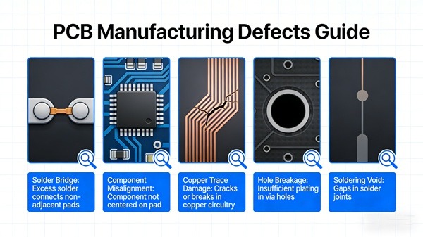
Via Defeitos
Descrição:
Falha elétrica ou mecânica de orifícios ou vias metalizados.
Causas comuns:
- Revestimento de cobre incompleto
- Mancha ou detritos da broca
- Rachaduras na parede do furo
Prevenção:
- Parâmetros de perfuração otimizados
- Processo de galvanização estável
- Inspeção transversal
Desalinhamento da máscara de solda
Descrição:
As aberturas da máscara de solda não se alinham com as almofadas ou traços.
Causas comuns:
- Desalinhamento da arte final
- Encolhimento do processo
- Controle de alinhamento inadequado
Prevenção:
- Calibração precisa da imagem
- Inspeção do alinhamento da máscara de solda
Quais etapas de fabricação causam a maioria dos defeitos em placas de circuito impresso?
Certas etapas de fabricação são estatisticamente mais propensas a introduzir defeitos.
| Etapa de fabricação | Defeitos típicos | Impacto |
|---|---|---|
| Gravação da camada interna | Abre, shorts | Problemas de integridade do sinal |
| Laminação | Delaminação, desalinhamento | Falha de confiabilidade |
| Perfuração | Por meio de defeitos | Conexões intermitentes |
| Revestimento | Cobre fino, vazios | Circuitos abertos |
| Máscara de solda | Desalinhamento | Perda de rendimento da montagem |
É por isso que fabricantes experientes concentram o controle de qualidade nessas etapas de alto risco.
Como o DFM reduz os defeitos de fabricação de PCBs
Um adequado Revisão DFM é a maneira mais eficaz de reduzir defeitos de fabricação antes do início da produção.
As principais considerações sobre DFM incluem:
- Ajustando a largura e o espaçamento dos traços à capacidade de fabricação
- Garantir o tamanho suficiente do anel anular
- Otimização da pilha para estabilidade da laminação
- Evitar tolerâncias restritas desnecessárias
At TOPFASTCada pedido de PCB é submetido a uma análise DFM para identificar antecipadamente potenciais riscos de defeitos, reduzindo retrabalhos e atrasos na produção.
Medidas de controle de qualidade na TOPFAST
Como fabricante profissional de PCB, a TOPFAST aplica controle de qualidade em todo o processo de fabricação:
- Inspeção Ótica Automatizada (AOI)
- Inspeção por raios X para estruturas HDI
- Teste elétrico com sonda voadora
- Conformidade com IPC Classe 2 / Classe 3
- Inspeção visual e dimensional final
Essa abordagem de inspeção em várias camadas garante que os defeitos sejam detectados e corrigidos antes do envio.
Como os defeitos de fabricação de placas de circuito impresso afetam a montagem e a confiabilidade
Os defeitos de fabricação muitas vezes causam problemas sérios durante a montagem de placas de circuito impresso, incluindo:
- Baixa soldabilidade
- Baixo rendimento de BGA
- Tombstoning ou bridging
- Falhas precoces em campo
A fabricação de PCB de alta qualidade é essencial para o desempenho estável do PCBA e a confiabilidade do produto a longo prazo.
Conclusão
PCB manufacturing defects are not random events—they are predictable and preventable when design and process are properly controlled.
Ao combinar uma análise minuciosa do DFM, processos de fabricação controlados e padrões de inspeção rigorosos, TOPFAST ajuda os clientes a minimizar defeitos de fabricação de placas de circuito impresso e a obter resultados consistentes e confiáveis, desde a fase de protótipo até a produção em massa.
Perguntas frequentes (FAQ)
R: Circuitos abertos e curtos-circuitos são os defeitos mais comuns, geralmente causados por problemas de gravação ou revestimento.
R: Embora nenhum processo seja 100% livre de defeitos, uma revisão adequada do DFM e um controle de qualidade rigoroso podem reduzir significativamente as taxas de defeitos.
R: Os projetistas devem seguir as diretrizes de DFM, evitar tolerâncias restritas desnecessárias e trabalhar em estreita colaboração com fabricantes experientes de PCB.
R: Alguns defeitos são visíveis através da inspeção, enquanto outros requerem testes elétricos para serem detectados.