Índice
1. Introdução às placas de circuito impresso e aos componentes principais
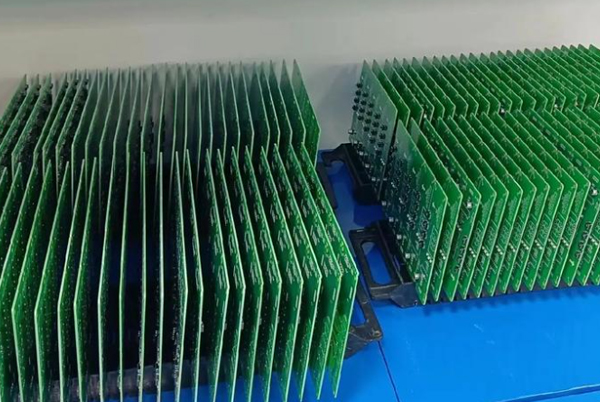
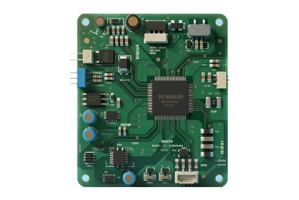
Placas de circuito impresso (PCBs) são componentes fundamentais na indústria eletrônica. Suas principais funções incluem: transmissão de sinal, apoio físico, distribuição de energiae gestão térmica. Uma PCB é composta por vários elementos especializados: o camada de serigrafia (Sobreposição) para identificação de componentes, acabamentos de superfície (como ENIG, HASL), vias para conexões elétricas entre camadas, Componentes de furo passante (PTH) e Dispositivos de montagem em superfície (SMD), cobre derramado (Polígono), almofadas térmicas de alívio, traços de sinal (Pista) e almofadas, entre outras características essenciais.
2. Sistema de classificação de PCB
2.1 Classificação por material do substrato
Substratos de cerâmica: Utilizing materials like Alumina (Al₂O₃), Aluminum Nitride (AlN), or Silicon Carbide (SiC), these offer exceptional thermal conductivity and are designed for high-temperature environments and high-power applications.
PCBs com núcleo metálico (MCPCBs): Incluindo substratos à base de alumínio e cobre, conhecidos pela sua dissipação de calor superior, amplamente utilizados em circuitos de alta potência e iluminação LED.
Substratos à base de papel: Como os tipos FR-1 e FR-2, utilizam papel de fibra como reforço, impregnado com resina e laminado com folha de cobre, adequado principalmente para placas de um ou dois lados.
Substratos compostosCombinar de forma inovadora as características de vários materiais, por exemplo, CEM-2 (resina epóxi com núcleo de papel e superfícies de tecido de vidro), para atender a requisitos de desempenho específicos.
2.2 Classificação por características estruturais
PCBs rígidos: Use substratos rígidos não flexíveis, incluindo vários tipos, como FR-4 (epóxi de vidro), à base de papel, compósitos, cerâmicos e placas com núcleo metálico.
PCBs flexíveis (PCBs flexíveis): Utilizam substratos isolantes flexíveis, permitindo dobrar, enrolar e dobrar, ideais para as restrições de espaço dos dispositivos eletrônicos portáteis.
PCBs rígidas e flexíveis: Integre de forma inteligente zonas rígidas e zonas flexíveis, oferecendo resistência estrutural e flexibilidade de instalação.
PCBs HDI (Interconexão de alta densidade): Utiliza tecnologia microvia e folhas de cobre ultrafinas para atender às demandas de miniaturização dos dispositivos eletrônicos. As estruturas incluem vias empilhadas em duas etapas, vias escalonadas em duas etapas e HDI em uma etapa.
Substratos IC: Projetado especificamente para embalagens de chips, fornecendo funções essenciais como conexão elétrica, proteção física, suporte estrutural e gerenciamento térmico.
3. Análise aprofundada da tecnologia de substratos PCB
3.1 Estrutura de empilhamento de camadas
As placas de circuito impresso modernas apresentam um design multicamadas:
- Núcleo: Laminado composto por tecido de fibra de vidro e resina epóxi, revestido com cobre em ambos os lados.
- Pré-impregnado (Pré-impregnado): Um composto de tecido de fibra de vidro e resina parcialmente curada, responsável pela ligação das camadas durante a laminação.
- Folha de cobre: Divided into Electro-Deposited (ED) copper (preferred for rigid boards) and Rolled Annealed (RA) copper (used for flexible boards). Thickness is measured in ounces (OZ), e.g., 1 OZ (≈35µm).
3.2 Via Technologies
As vias de interconexão de PCB são classificadas em três tipos:
- Via de furo passante: Passa por todas as camadas do circuito.
- Via cega: Conecta uma camada externa a uma ou mais camadas internas, mas não atravessa toda a placa.
- Enterrado via: Localizado inteiramente nas camadas internas, conectando duas ou mais camadas internas sem atingir as superfícies externas.
3.3 Parâmetros-chave de desempenho
Parâmetros térmicos:
- Tg (Temperatura de transição vítrea): O ponto crítico em que a resina passa de um estado rígido para um estado mais macio, afetando diretamente a resistência ao calor do substrato.
- Td (Temperatura de decomposição): A temperatura na qual a resina perde 5% de sua massa devido à degradação térmica.
- CTE (Coefficient of Thermal Expansion): Determines dimensional stability under temperature variations. Typically X/Y: 16-18 ppm/°C, Z: 40-60 ppm/°C.
Parâmetros elétricos:
- Dk (Dielectric Constant): Influences signal propagation speed and characteristic impedance. A lower Dk generally allows faster signal speed (V = C/√Dk).
- Df (Fator de dissipação): Afeta a integridade e a qualidade do sinal; um Df mais baixo significa menos perda de sinal.
- Resistividade superficial/volumétrica: mede o desempenho condutivo.
Parâmetros mecânicos:
- Resistência à flexão e resistência ao descolamento
- Absorção de água: afeta a estabilidade e a confiabilidade do substrato. A umidade pode aumentar o Dk e o risco de delaminação (“popcorning”).
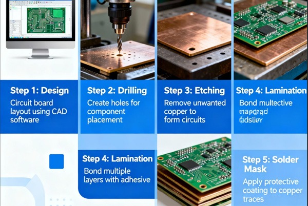
4. Fluxo do processo de fabricação de placas de circuito impresso de precisão
A fabricação de placas de circuito impresso segue uma sequência rigorosa:
- Aquisição de imagens da camada interna → 2. Laminação fotorresistente → 3. Exposição → 4. Desenvolvimento → 5. Gravura → 6. Resistência à tira → 7. Empilhamento de camadas → 8. Laminação → 9. Perfuração → 10. Revestimento (PTH) → 11. Laminação resistente da camada externa → 12. Exposição → 13. Desenvolvimento → 14. Revestimento padrão (Cu/Sn) → 15. Resistência à tira → 16. Gravura → 17. Tira de estanho → 18. Serigrafia/Impressão de legendas → 19. Acabamento da superfície
5. Comparação abrangente dos tratamentos de acabamento de superfícies
| Acabamento da superfície | Principais características e vantagens | Limitações/Desafios | Nível de custo | Thickness Range (µm) | Prazo de validade |
|---|---|---|---|---|---|
| HASL (sem chumbo) | Adequado para almofadas grandes, espaçamento amplo | Não é ideal para HDI; alta temperatura; superfície irregular | Médio-Alto | 2-5 (no bloco) | 12 meses |
| HASL (à base de chumbo) | Excelente resistência mecânica | Preocupação ambiental (teor de Pb) | Médio-Alto | 2-5 (no bloco) | 12 meses |
| OSP | Processo simples, baixo custo | Não adequado para múltiplas refluxos; inspeção difícil | Mais baixo | 0.1 – 0.5 | 6 meses |
| ENIG (Níquel químico/Ouro por imersão) | Soldagem confiável, superfície plana, boa resistência à corrosão | Potencial para “Black Pad” (corrosão do níquel), “Gold Embrittlement” (fragilização do ouro) | Alta | Ni: 3-5 / Au: 0,03-0,08 | 12 meses |
| ENEPIG (Ni/Pd/Au por imersão sem eletricidade) | Aplicativos de ponta, resistência superior à corrosão, soldável por fio | Controle complexo do processo, potencial para manchas pretas/descoloração | Alta | Ni: 2-5 / Pd: 0,05-0,15 / Au: 0,05-0,15 | 6 meses |
| Prata por imersão (ImAg) | Superfície plana, adequada para múltiplas refluxões | Mancha facilmente, requer condições rigorosas de armazenamento | Médio | 0.1 – 0.5 | 12 meses |
| Estanho de imersão (ImSn) | Boa planicidade, soldabilidade | Risco de formação de cristais de estanho, baixa resistência ao envelhecimento térmico | Baixa | 0.8 – 1.2 | 6 meses |
| Ni/Au eletrolítico (Ouro macio) | Excelente resistência ao desgaste, confiabilidade de contato | Alto consumo de ouro, possíveis problemas de aderência da máscara de solda no ouro | Mais alto | Ni: 3-5 / Au: ≥0.05 (selective) | 12 meses |
| Ouro duro eletrolítico | Resistência extrema ao desgaste (por exemplo, para os dedos) | Custo mais elevado, processo mais complexo | Mais alto | 0,3 – 3,0 (em contato) | 12 meses |