V-scoring, a critical process in placa de circuito impresso (PCB) manufacturing, plays a vital role in improving production efficiency and reducing manufacturing costs. This article will provide a systematic professional analysis of the technical principles, design standards, and implementation essentials of V-scoring, offering practical reference for electronics engineers, hardware developers, and manufacturing technicians.
Índice
Technical Principles and Process Characteristics of V-Scoring
1.1 Technical Definition and Physical Mechanism
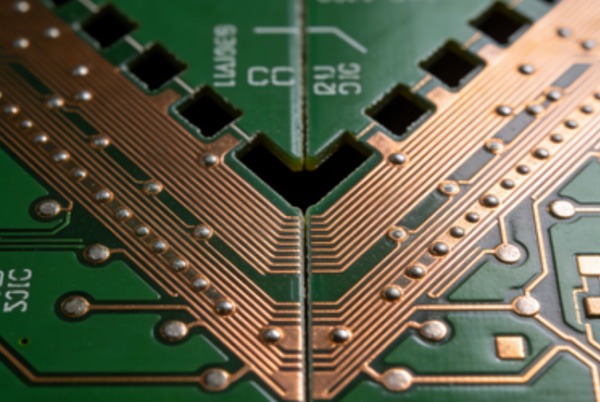
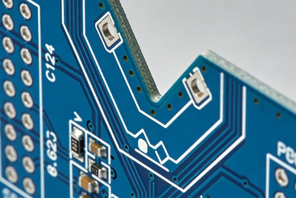
V-scoring is a process where specialized CNC equipment cuts V-shaped grooves at specific angles on the top and bottom surfaces of a PCB panel, leaving a precisely controlled connecting layer. This enables panelized assembly and controlled separation. Its physical principle is based on the stress concentration effect in material mechanics: the V-shaped groove creates a geometric discontinuity, generating stress concentration under bending moments, thus enabling clean separation along the predetermined path.
1.2 Process Parameter System
Professional V-scoring involves the coordinated control of multiple parameters:
- Cutter Angle: Standard angles are 30°, 45°, and 60°. The selection depends on board thickness and material properties.
- Cutting Depth: Typically set to between 1/3 and 2/3 of the board thickness, with symmetrical cuts on top and bottom.
- Remaining Thickness: A critical parameter, generally controlled within the range of 0.2±0.05mm to 0.4±0.05mm.
- Cutting Speed: Adjusted according to material type. For FR-4 material, a speed of 2-4 m/min is recommended.
1.3 Material Suitability Analysis
Different substrate materials exhibit varying responses to V-scoring:
| Tipo de material | Cutting Characteristics | Recommended Remaining Thickness | Precauções |
|---|---|---|---|
| Standard FR-4 | Excellent cutting performance, clean edges | 1/3 of the board thickness | Control glass fiber layer delamination |
| High-Frequency Boards | Higher brittleness requires reduced cutting speed | 40% of board thickness | Prevent dielectric layer cracking |
| Metal Core Boards | Requires special cutters and cooling systems | 35% of board thickness | Avoid aluminum chip contamination |
| Flexible Circuits | Not suitable for standard V-scoring | – | Routing separation is recommended |
Professional Panelization Design Guidelines and Engineering Standards
2.1 Panel Layout Optimization Strategy
Geometric Constraints:
- Minimum panel spacing: ≥0.3mm (considering tool tolerance and thermal expansion)
- Panel direction: All separation lines should maintain parallel or perpendicular relationships
- Panel utilization rate: Target ≥85%, balancing material cost and process feasibility
Electrical Design Considerations:
- High-frequency signal line distance from groove edge: ≥3mm (to prevent impedance discontinuity)
- Power plane segmentation: Avoid segmentation across V-grooves to ensure current path integrity
- Ground continuity: Design cross-groove jumpers if necessary
2.2 Component Layout Protection Guidelines
Keep-out Area Definition:
- Standard components: ≥1.5mm from V-groove centerline
- Ceramic components: ≥2.0mm from groove edge (to prevent mechanical stress damage)
- BGA packages: ≥3.0mm from groove edge (to avoid solder joint fatigue)
- Tall components (>5mm): Distance from groove edge ≥ component height (to prevent interference)
2.3 Design File Preparation Specifications
Manufacturing File Requirements:
- Gerber files must include a clearly defined V-Cut layer.
- Provide a panelization diagram indicating cut lines and direction.
- Clearly specify the tolerance requirements for the remaining thickness.
- Annotate board material type and thickness specifications.
Professional Manufacturing Process and Quality Control
3.1 Standardized Process Flow
Panel Preprocessing → Optical Alignment → Top Surface Scoring → Panel Flipping & Alignment →
Bottom Surface Scoring → Depth Inspection → Cleaning → Final Inspection
3.2 Critical Process Control Points
Alignment Accuracy Control:
- Use high-precision optical alignment systems (±0.02mm)
- Design dedicated fiducial marks
- Implement the first article 3D profile inspection
Tool Management System:
- Regular tool wear inspection (check after every 500 meters of cutting)
- Multi-tool automatic switching system
- Real-time cutting depth feedback adjustment
3.3 Quality Inspection Standards
AQL Inspection Items:
- Groove depth accuracy: ±0.05mm
- Groove width consistency: CV ≤ 5%
- Remaining thickness uniformity: ±0.03mm
- Edge quality: No glass fiber delamination, no copper foil lifting
Professional Manufacturing Advantages: TOPFAST’s Engineering Capabilities
As a professional PCB manufacturing service provider, TOPFAST possesses the following engineering and technical advantages in the field of V-scoring:
4.1 Advanced Equipment Configuration
- Utilizes German SCHUNK CNC V-scoring systems with ±0.01mm repeatability.
- Equipped with online 3D scanning inspection systems for real-time scoring quality monitoring.
- Integrated automatic cleaning units ensure no residue remains in the grooves.
4.2 Process Optimization Capabilities
Provides customized solutions for special requirements:
- High-Density Panelization Solutions: Precision panelization with minimum spacing down to 0.2mm.
- Mixed-Material Panelization: Technology for panelizing PCBs of different materials.
- Pre-set Stress Relief: Reduces separation stress by optimizing scoring parameters.
4.3 Engineering Support Services
- DFM (Design for Manufacturability) analysis to identify panelization risks early.
- Free panelization optimization suggestions.
- Rapid prototype verification service.
Comparative Analysis of V-Scoring vs. Other Depaneling Techniques
| Technical Indicator | V-Scoring | Tab Routing | Routing Separation | Laser Cutting |
|---|---|---|---|---|
| Edge Quality | Good | Ruim | Excelente | Excelente |
| Production Efficiency | Alta | Médio | Baixa | Médio |
| Equipment Investment | Médio | Baixa | Alta | Alta |
| Suitable Shapes | Straight lines | Any | Any | Any |
| Material Waste | Baixa | Baixa | Médio | Very Low |
| Aplicação típica | High-volume rectangular boards | Low-volume irregular boards | Boards with high-quality requirements | Precision flexible boards |
Analysis of Common Engineering Issues and Solutions
6.1 Poor Depaneled Edge Quality
Symptom: Glass fiber layer delamination or copper foil tearing.
Root Cause: Dull tools or improper cutting parameters.
Solutions:
- Implement a preventive tool replacement schedule.
- Optimize cutting speed and feed rate parameters.
- Adjust the tool angle for special materials.
6.2 Component Failure Due to Depaneling Stress
Symptom: Ceramic capacitor cracking or BGA solder joint micro-cracking.
Engineering Analysis: Dynamic stress during depaneling exceeds component tolerance limits.
Control Measures:
- Increase the safe distance between components and groove edges.
- Use progressive depaneling fixtures.
- Optimize panel layout to avoid high-stress areas.
Industry Trends and Technological Outlook
7.1 Intelligent Manufacturing Upgrades
- Machine learning-based adaptive adjustment of cutting parameters.
- Real-time monitoring systems and predictive maintenance.
- Application of digital twin technology in process optimization.
7.2 New Material Adaptation Innovations
- V-scoring process optimization for high-frequency, high-speed laminates.
- Micro V-scoring technology for ultra-thin multilayer boards.
- Precision separation solutions for ceramic substrates.
7.3 Sustainable Development Directions
- Panelization algorithm optimization to reduce material waste.
- Development of energy-efficient scoring equipment.
- V-scoring process compatibility with recyclable materials.
Professional Recommendations and Engineering Practice Guidelines
For projects prioritizing reliability and consistency, we recommend:
- Early Design Involvement: Consider panelization solutions during the PCB layout phase to avoid later modifications.
- Rigorous Validation Process: Verify depaneling results with small-batch prototypes, paying special attention to edge-sensitive components.
- Choosing Professional Manufacturing: Projects with complex requirements or high reliability needs should select manufacturers with robust quality systems.
Leveraging extensive engineering experience, TOPFAST provides customers with comprehensive technical support from design review to mass production optimization. Our engineering team can assist in developing optimal panelization strategies, balancing efficiency, cost, and quality requirements to ensure each circuit board meets the intended technical specifications.
In today’s era of increasingly sophisticated electronics manufacturing, professional V-scoring technology is not only a guarantee of production efficiency but also a crucial foundation for product quality. Choosing a professional partner allows technological innovation and manufacturing processes to perfectly integrate, jointly driving progress and development in the electronics industry.