يمكن أن تؤثر عيوب تصنيع ثنائي الفينيل متعدد الكلور بشكل كبير على موثوقية المنتج والأداء الكهربائي والإنتاجية الإجمالية للتصنيع.
حتى العيوب الصغيرة التي تحدث أثناء التصنيع قد تؤدي إلى فشل وظيفي أثناء التجميع أو التشغيل الميداني.
في هذه المقالة، توب فاست, a professional PCB manufacturer, explains the most common PCB manufacturing defects, why they occur, and—most importantly—how to prevent them through proper design and manufacturing control.
جدول المحتويات
ما هي عيوب تصنيع ثنائي الفينيل متعدد الكلور؟
عيوب تصنيع PCB هي عيوب مادية أو كهربائية غير مقصودة تحدث أثناء عملية التصنيع.
قد تحدث هذه العيوب بسبب قيود التصميم أو مشاكل المواد أو عدم استقرار العملية أو عدم كفاية مراقبة الجودة.
على عكس المشاكل المتعلقة بالتجميع، توجد عيوب التصنيع في PCB فقط قبل تركيب أي مكونات.
لماذا تحدث عيوب تصنيع ثنائي الفينيل متعدد الكلور
تنجم معظم عيوب لوحات الدوائر المطبوعة عن واحد أو أكثر من العوامل التالية:
- غير كافٍ سوق دبي المالي (تصميم قابل للتصنيع) مراجعة
- تفاوتات تصميمية ضيقة تتجاوز قدرة العملية
- تناقضات مادية
- تباين العملية أثناء الحفر أو التصفيح أو الطلاء
- عدم كفاية عمليات الفحص أو الاختبار
الفهم أي خطوة من خطوات التصنيع تؤدي إلى ظهور أي عيب هو مفتاح الوقاية.
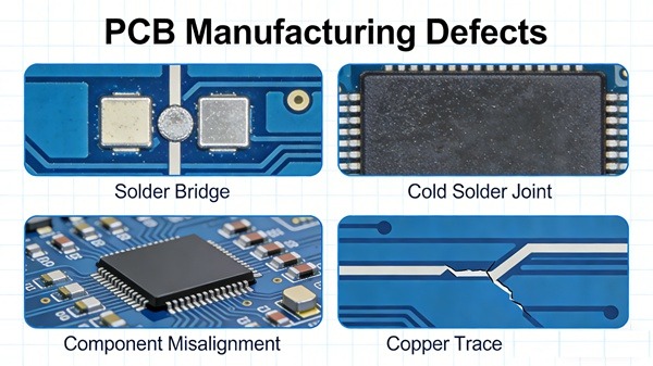
أكثر عيوب تصنيع لوحات الدوائر المطبوعة شيوعًا
فيما يلي أكثر عيوب تصنيع لوحات الدوائر المطبوعة شيوعًا في بيئات الإنتاج الفعلية.
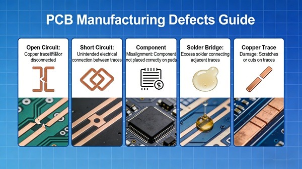
الدوائر المفتوحة
الوصف:
انقطاع في مسار النحاس يقطع الاستمرارية الكهربائية.
الأسباب الشائعة:
- الحفر الزائد أثناء معالجة الطبقة الداخلية أو الخارجية
- طلاء نحاسي رقيق في الثقوب
- الأضرار الميكانيكية أثناء المناولة
الوقاية:
- تصميم عرض التتبع المناسب
- معلمات الحفر المتحكم بها
- سمك طلاء النحاس المناسب
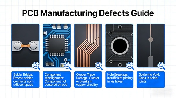
الدوائر القصيرة
الوصف:
توصيلات كهربائية غير مقصودة بين الموصلات المتجاورة.
الأسباب الشائعة:
- تباعد غير كافٍ بين الآثار
- اختلال قناع اللحام
- بقايا النحاس بعد الحفر
الوقاية:
- التحقق من تباعد DFM
- تسجيل دقيق لقناع اللحام
- فحص الهيئة العربية للتصنيع
تقشر
الوصف:
انفصال طبقات PCB بسبب ضعف الترابط.
الأسباب الشائعة:
- درجة حرارة أو ضغط تصفيح غير مناسبين
- الرطوبة المحبوسة في المواد
- اختيار رقائق غير متوافقة
الوقاية:
- عملية التصفيح المتحكم فيها
- التخزين السليم للمواد والخبز
- اختيار المواد المناسبة ذات درجة حرارة انصهار عالية
عن طريق العيوب
الوصف:
عطل كهربائي أو ميكانيكي في الثقوب المطلية أو المسارات.
الأسباب الشائعة:
- طلاء نحاسي غير مكتمل
- مسحة أو بقايا الحفر
- تشقق جدار الحفرة
الوقاية:
- معلمات الحفر المُحسّنة
- عملية طلاء مستقرة
- فحص المقطع العرضي
اختلال قناع اللحام
الوصف:
فتحات قناع اللحام لا تتوافق مع الوسادات أو المسارات.
الأسباب الشائعة:
- سوء تسجيل الأعمال الفنية
- انكماش العملية
- التحكم غير الكافي في المحاذاة
الوقاية:
- معايرة دقيقة للتصوير
- فحص محاذاة قناع اللحام
ما هي خطوات التصنيع التي تسبب معظم عيوب PCB؟
بعض خطوات التصنيع أكثر عرضة لإحداث عيوب من الناحية الإحصائية.
| خطوة التصنيع | العيوب النموذجية | التأثير |
|---|---|---|
| حفر الطبقة الداخلية | يفتح، شورتات | مشاكل سلامة الإشارة |
| التصفيح | تقشر، سوء التسجيل | فشل الموثوقية |
| الحفر | عن طريق العيوب | اتصالات متقطعة |
| التصفيح | نحاس رقيق، فراغات | الدوائر المفتوحة |
| قناع اللحام | اختلال المحاذاة | خسارة إنتاجية التجميع |
هذا هو السبب في أن الشركات المصنعة ذات الخبرة تركز مراقبة الجودة على هذه المراحل عالية المخاطر.
كيف تقلل DFM من عيوب تصنيع ثنائي الفينيل متعدد الكلور
مناسب مراجعة DFM هي الطريقة الأكثر فعالية لتقليل عيوب التصنيع قبل بدء الإنتاج.
تشمل الاعتبارات الرئيسية لـ DFM ما يلي:
- مطابقة عرض التتبع والمسافة مع قدرة التصنيع
- ضمان حجم حلقة حلقي كافٍ
- تحسين التراص من أجل استقرار التصفيح
- تجنب التفاوتات الضيقة غير الضرورية
At توب فاست، تخضع كل طلبية من لوحات الدوائر المطبوعة لتحليل DFM لتحديد مخاطر العيوب المحتملة في وقت مبكر، مما يقلل من إعادة العمل وتأخير الإنتاج.
تدابير مراقبة الجودة في TOPFAST
بصفتها شركة تصنيع PCB محترفة، تطبق TOPFAST مراقبة الجودة طوال عملية التصنيع:
- الفحص البصري الآلي (AOI)
- الفحص بالأشعة السينية للهياكل HDI
- اختبار كهربائي بمسبار طائر
- التوافق مع IPC الفئة 2 / الفئة 3
- الفحص النهائي للبعد البصري والأبعاد
يضمن نهج الفحص متعدد الطبقات هذا اكتشاف العيوب وتصحيحها قبل الشحن.
كيف تؤثر عيوب تصنيع ثنائي الفينيل متعدد الكلور على التجميع والموثوقية
غالبًا ما تؤدي عيوب التصنيع إلى مشاكل خطيرة أثناء تجميع لوحات الدوائر المطبوعة، بما في ذلك:
- ضعف قابلية اللحام
- انخفاض إنتاجية BGA
- تومبستونينغ أو بريدجينغ
- أعطال ميدانية مبكرة
يعد تصنيع لوحات الدوائر المطبوعة عالية الجودة أمرًا ضروريًا لأداء PCBA المستقر وموثوقية المنتج على المدى الطويل.
الخاتمة
PCB manufacturing defects are not random events—they are predictable and preventable when design and process are properly controlled.
من خلال الجمع بين المراجعة الشاملة لتصميم التصنيع (DFM) وعمليات التصنيع الخاضعة للرقابة ومعايير الفحص الصارمة، توب فاست يساعد العملاء على تقليل عيوب تصنيع ثنائي الفينيل متعدد الكلور إلى الحد الأدنى وتحقيق نتائج متسقة وموثوقة من النموذج الأولي إلى الإنتاج الضخم.
الأسئلة الشائعة (FAQ)
ج: الدوائر المفتوحة والدوائر القصيرة هي العيوب الأكثر شيوعًا، وغالبًا ما تنتج عن مشكلات في الحفر أو الطلاء.
ج: على الرغم من أنه لا توجد عملية خالية من العيوب بنسبة 100٪، إلا أن المراجعة السليمة لتصميم قابلية التصنيع (DFM) ومراقبة الجودة الصارمة يمكن أن تقلل من معدلات العيوب بشكل كبير.
ج: يجب على المصممين اتباع إرشادات DFM، وتجنب التفاوتات الضيقة غير الضرورية، والعمل عن كثب مع مصنعي PCB ذوي الخبرة.
ج: بعض العيوب يمكن رؤيتها من خلال الفحص، بينما تتطلب عيوب أخرى إجراء اختبارات كهربائية للكشف عنها.