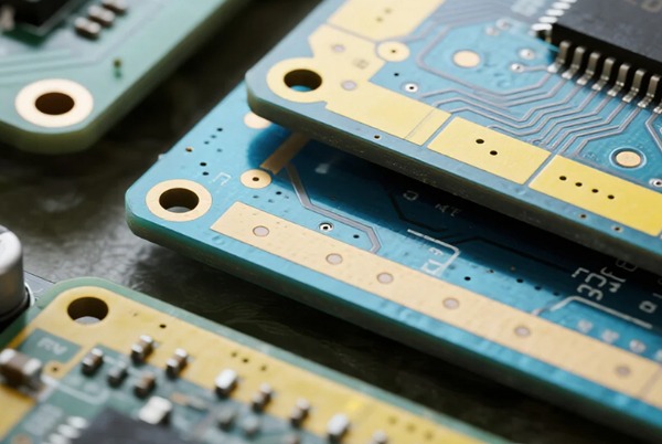
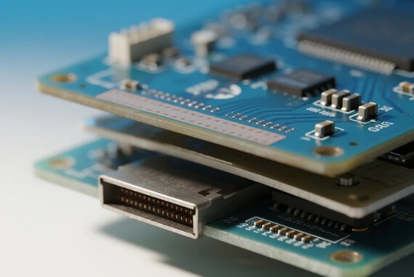
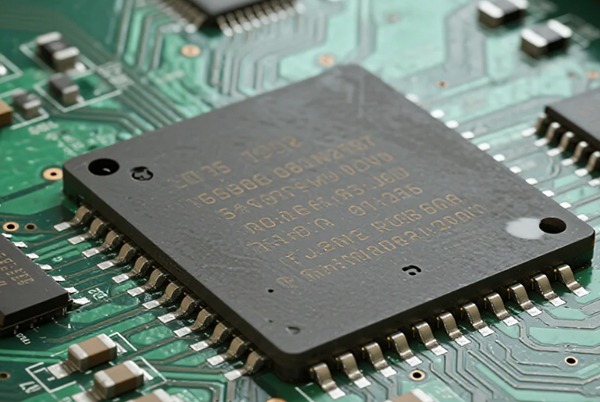
لوحات الدوائر المطبوعة (PCBs) هي الناقلات الأساسية للأجهزة الإلكترونية. يؤثر عدد الطبقات الموجودة فيها بشكل مباشر على كفاءة عمل المنتج وتكلفته وموثوقيته. ستتناول هذه المقالة الحدود النظرية لعدد طبقات PCB، والأمور العملية التي تجعل تصنيعها صعبًا، ومقارنتها عند النظر إلى مزايا وعيوب عدد الطبقات المختلفة، والأمور التقنية التي يجب مراعاتها عند اختيار عدد الطبقات المناسب. وستوفر مرجعًا كاملاً للمهندسين الإلكترونيين ومصممي المنتجات.
جدول المحتويات
I. الحدود النظرية والقيود العملية لتصنيع طبقات PCB
حدود الطبقة النظرية
هناك لا يوجد حد أقصى مطلق إلى عدد الطبقات في لوحة الدوائر المطبوعة. مع التقدم في تكنولوجيا الإلكترونيات الدقيقة، قامت الشركات المصنعة العالمية الرائدة مثل إنتل وسامسونج حققت إنتاجًا ضخمًا من ثنائي الفينيل متعدد الكلور مع أكثر من 100 طبقة، وذلك بشكل أساسي للتطبيقات المتخصصة مثل أجهزة الكمبيوتر العملاقة والخوادم المتطورة ومعدات الفضاء الجوي.
قيود التصنيع العملية
على الرغم من الإمكانية النظرية، يواجه الإنتاج الضخم العملي عدة قيود:
- القيود التقنية: تتزايد متطلبات دقة المحاذاة بين الطبقات بشكل كبير مع إضافة طبقات جديدة.
- القيود المادية: تتطلب لوحات الدوائر المطبوعة ذات الطبقات العالية مواد عالية الاستقرار ذات معاملات تمدد حراري منخفضة.
- قيود التكلفة: يمكن أن تبلغ تكلفة تصنيع لوحة PCB ذات 32 طبقة 5-8 أضعاف تكلفة لوحة ذات 4 طبقات.
- قيود الغلة: بعد 20 طبقة، كل طبقة إضافية تقلل العائد بنسبة 2-3٪ تقريبًا.
نطاقات طبقة الإنتاج القياسية
يوضح الجدول أدناه التوزيعات النموذجية لطبقات PCB عبر مختلف مجالات التطبيق:
| مجال التطبيق | الطبقات النموذجية | المنتجات التمثيلية | الخصائص التقنية |
|---|---|---|---|
| الإلكترونيات الاستهلاكية | 4-8 طبقات | الهواتف الذكية والأجهزة اللوحية | حساسة للتكلفة، محدودة المساحة |
| معدات الاتصالات | 8-16 طبقة | محطات قاعدة 5G، محولات الشبكة | متطلبات إدارة حرارية عالية التردد وعالية السرعة |
| التحكم الصناعي | 6-14 طبقات | PLCs، اللوحات الأم الصناعية | موثوقية عالية، ومناعة قوية ضد التداخل |
| الحوسبة المتطورة | 12-32 طبقة | الخوادم، بطاقات مسرع الذكاء الاصطناعي | كثافة فائقة، نقل عالي السرعة |
| المجالات المتخصصة | 32-100+ طبقة | أجهزة الكمبيوتر العملاقة، معدات الفضاء الجوي | أداء فائق، مواد خاصة |
ثانياً: تحليل شامل لمزايا لوحات الدوائر المطبوعة متعددة الطبقات
1. قدرة تكامل عالية الكثافة
من خلال تصميم التكديس الطبقي، لوحات الدوائر المطبوعة متعددة الطبقات تحسين كثافة الأسلاك بشكل كبير في المساحات المحدودة. تظهر بيانات الاختبار أن اللوحات ذات 8 طبقات توفر كثافة أسلاك أعلى بنسبة 60٪ تقريبًا من اللوحات ذات 4 طبقات، بينما يمكن للوحات ذات 16 طبقة تحسين الكثافة بنسبة تزيد عن 120٪.
2. سلامة إشارة ممتازة
من خلال التصميم المناسب للتكديس والتحكم في المعاوقة، تضمن لوحات الدوائر المطبوعة متعددة الطبقات بشكل فعال جودة نقل الإشارات عالية السرعة:
- ألواح من 4 طبقات: تقليل توهين الإشارة بأكثر من 40٪ مقارنة باللوحات ذات الوجهين بتردد 1 جيجاهرتز
- ألواح ذات 8 طبقات: دعم واجهات عالية السرعة مثل PCIe 4.0 بمعدلات نقل تصل إلى 16 جيجابت/ثانية
- ألواح ذات 16 طبقة أو أكثر: Support 56Gbps and above high-speed serial transmission with bit error rates below 10⁻¹²
3. توافق كهرومغناطيسي فائق (EMC)
توفر لوحات الدوائر المطبوعة متعددة الطبقات حماية كهرومغناطيسية طبيعية من خلال تصميمات كاملة للأرضية ومستوى الطاقة:
- عندما تزيد تغطية المستوى الأرضي عن 85٪، يمكن تقليل الإشعاع الكهرومغناطيسي بمقدار 12-15 ديسيبل.
- يقلل فصل طبقات الطاقة/الأرض عن طبقات الإشارة من التداخل الكهرومغناطيسي بين الطبقات بأكثر من 20 ديسيبل.
4. أداء حراري فعال
- Dedicated thermal layer designs can reduce chip junction temperature by over 18℃
- Aluminum substrates achieve thermal conductivity coefficients of 2.2W/m·K, 3-5 times better than traditional FR-4 material
5. مرونة التصميم وتحسين المساحة
- 10-layer HDI boards can reduce smartphone motherboard size to 5cm×5cm, saving 70% space compared to traditional solutions
- تدعم مساحة الأسلاك ثلاثية الأبعاد تصميمات الدوائر الأكثر تعقيدًا
ثالثاً: التحديات والقيود التي تواجهها لوحات الدوائر المطبوعة متعددة الطبقات
تحليل تكاليف التصنيع
يحافظ عدد طبقات PCB والتكلفة على علاقة نمو غير خطية:
| الطبقات | التكلفة النسبية | العوامل الرئيسية المؤثرة على التكلفة |
|---|---|---|
| 2-طبقة 2 | 1.0x | المواد الأساسية، العمليات البسيطة |
| 4 طبقات | 1.8-2.5x | زيادة دورات التصفيح، متطلبات محاذاة أعلى |
| 6 طبقات | 3-4x | زيادة تعقيد عمليات الحفر، وانخفاض الإنتاجية |
| 8 طبقات | 4-6x | ارتفاع تكاليف المواد، وزيادة تعقيد العمليات |
| 16 طبقة | 8-12x | متطلبات خاصة للمعدات، وزيادة كبيرة في تكاليف الاختبار |
دورات إنتاج ممتدة
يتطلب تصنيع لوحات الدوائر المطبوعة متعددة الطبقات عمليات متعددة من التصفيح والحفر والطلاء:
- المهلة القياسية للوحات ذات 4 طبقات: 5-7 أيام
- المهلة القياسية للوحة ذات 8 طبقات: 10-14 يومًا
- المهلة القياسية للوحة ذات 16 طبقة: 15-25 يومًا
- المهلة القياسية للوحة ذات 32 طبقة: 30-45 يومًا
تحديات الاختبار والإصلاح
- تتطلب لوحات الدوائر المطبوعة ذات الطبقات العالية طرق اختبار متعددة، بما في ذلك اختبار المسبار المتحرك والفحص بالأشعة السينية.
- صعوبة تحديد موقع العطل الداخلي، وعادة ما تقل نسبة نجاح إصلاح حزم BGA عن 30٪.
- يمكن أن تمثل تكاليف الاختبار 15-20٪ من إجمالي تكاليف التصنيع
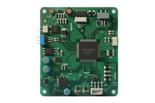
IV. منهجية اختيار طبقة PCB وإرشادات التصميم
عوامل تحديد الطبقة الرئيسية
- التعقيد الوظيفي: عدد خطوط الإشارة هو مؤشر رئيسي
- أقل من 50 سطراً: يمكن النظر في استخدام لوحات على الوجهين
- 50-200 خط: لوحات موصى بها ذات 4 طبقات
- >200 خط: يتطلب 6 طبقات أو أكثر
- متطلبات تردد الإشارة
- <50 ميجاهرتز: قد تكفي اللوحات ذات الوجهين
- 50 ميجاهرتز-100 ميجاهرتز: لوحات موصى بها ذات 4 طبقات
- >100 ميجاهرتز: يجب استخدام 6 طبقات أو أكثر
- مستويات GHz: تتطلب 8 طبقات أو أكثر مع تصميم احترافي
- متطلبات توصيل حزمة BGA
- 0.65 مم: قد تكفي اللوحات ذات 4 طبقات
- مسافة 0.4 مم: يجب استخدام 6 طبقات أو أكثر
- لكل انخفاض بمقدار 0.1 مم في المسافة بين المسامير، يوصى بإضافة 1-2 طبقات توجيه.
تصميم هيكل مكدس محسّن
الهياكل الموصى بها للتكديس لعدد مختلف من الطبقات:
هيكل مفضل من 4 طبقات:
الجزء العلوي (الإشارة) - طبقة الأرضية - طبقة الطاقة - الجزء السفلي (الإشارة)هيكل مكون من 6 طبقات مُحسّن:
الجزء العلوي (الإشارة) - طبقة الأرضية - طبقة الإشارة - طبقة الإشارة - طبقة الطاقة - الجزء السفلي (الإشارة)هيكل متطور مكون من 8 طبقات:
طبقة الإشارة - طبقة الأرضية - طبقة الإشارة - طبقة الطاقة - طبقة الأرضية - طبقة الإشارة - طبقة الطاقة - طبقة الإشارةخامساً: التقنيات الرئيسية لزيادة طبقات ثنائي الفينيل متعدد الكلور
تقنيات التوصيل المتقدمة
- تقنية الحفر بالليزر
- UV laser enables 25μm microvia processing
- Precision up to ±5μm, supporting blind and buried via fabrication
- تقنية أي توصيل بين الطبقات (ALIVH)
- يحقق اتصالات رأسية بين أي طبقتين من خلال ثقوب مكدسة
- يحسن كثافة الاتصال بين الطبقات بنسبة 40٪
- تركيبات العمليات العمياء/المدفونة
- ثقوب عمياء: وصلات بين السطح والطبقة الداخلية، قطرها 0.05-0.3 مم
- ثقوب مدفونة: وصلات الطبقة الداخلية، مخفية تمامًا
الابتكارات المادية
- تقنية هجينة عالية التردد
- يجمع بين المواد عالية التردد (مثل Rogers) و FR-4
- يستخدم مواد عالية التردد لطبقات الإشارات الحرجة، ومواد FR-4 فعالة من حيث التكلفة للطبقات الأخرى
- مواد عازلة للكهرباء ذات خسارة منخفضة للغاية
- Rogers RO4835: خسارة عازلة تبلغ 0.0035 فقط عند 10 جيجاهرتز
- توهين الإشارة بنسبة 0.3% فقط على مسافة نقل تبلغ مترًا واحدًا
اختراقات العملية
- تقنية التصفيح المتدرج
- يستخدم هياكل تصفيح متماثلة للتحكم في الالتواء
- Interlayer alignment error ≤5μm
- تقنية ملء الطلاء
- تحقيق خلو من الفراغات عن طريق التعبئة باستخدام طلاء النبض
- نسبة عرض إلى ارتفاع التغطية العمياء 0.8:1
VI. حالات التطبيق واتجاهات التكنولوجيا
حالات التطبيق الناجحة
| منتج التطبيق | الطبقات | الميزات التقنية | تحسين الأداء |
|---|---|---|---|
| محطة قاعدة 5G من هواوي | 24 طبقة | حفر هجين عالي التردد + ليزر | تقليل تأخير الإشارة بنسبة 80٪ |
| كمبيوتر سيارات تسلا | 12 طبقة | مواد مقاومة للحرارة العالية + تبريد محسّن | Operating temperature -40℃~125℃ |
| اللوحة الأم لجهاز iPhone | 10 طبقات | أي طبقة HDI | تخفيض الحجم بنسبة 40٪ |
| بطاقة تسريع الذكاء الاصطناعي من NVIDIA | 16 طبقة | مواد ذات خسارة منخفضة للغاية | معدل نقل 112 جيجابت في الثانية |
اتجاهات التنمية المستقبلية
- زيادة مستمرة في الطبقة: تتجه الإلكترونيات الاستهلاكية نحو 12-16 طبقة، بينما تتجه الحوسبة المتطورة نحو 50+ طبقة.
- ابتكار المواد: تطوير مواد جديدة ذات ثابت عازل كهربائي <3.0، وعامل خسارة <0.002
- التكامل: تضمين المكونات السلبية والهوائيات وغيرها داخل لوحات الدوائر المطبوعة
- الإدارة الحرارية: Developing thermal materials with conductivity >5W/m·K
الخاتمة
يعد اختيار عدد طبقات PCB مهمة هندسية معقدة تتطلب تحقيق التوازن بين الأداء والتكلفة والموثوقية وجدوى التصنيع. من اللوحات البسيطة ذات الوجهين إلى اللوحات المعقدة التي تتجاوز 32 طبقة، لكل خيار سيناريوهات تطبيق ومتطلبات تقنية محددة. مع تقدم تقنيات مثل 5G والذكاء الاصطناعي وإنترنت الأشياء، سيستمر الطلب على لوحات PCB عالية الطبقات في النمو، مما يدفع تقنية PCB نحو كثافة أعلى وأداء أعلى وموثوقية أكبر.