
لوحات الدوائر المطبوعة (PCBs) هي الركائز الأساسية للأجهزة الإلكترونية الحديثة. مع اتجاه الأجهزة نحو ترددات أعلى وسرعات أعلى وتصغير الحجم، أصبح التصميم الممتاز لتخطيط PCB عاملاً حاسماً في تحديد أداء المنتج. تتعمق هذه المقالة في تقنيات تخطيط PCB المتقدمة مثل التوجيه عالي السرعة والتحكم في المعاوقة وتحسين سلامة الطاقة، مما يساعد المهندسين على تصميم لوحات دوائر أكثر موثوقية وكفاءة.
جدول المحتويات
تقنية التوجيه عالي السرعة
مبدأ التتبع القصير والمباشر
يجب أن يتبع توجيه الإشارات عالية السرعة ما يلي مبدأ الشومسار اختبار، مما يقلل من الانحناءات والانعطافات غير الضرورية. الحفاظ على هندسة تتبع متسقة يقلل بشكل كبير من خطر تأخير الإشارة وتشويهها.
نقاط التنفيذ الرئيسية:
- إعطاء الأولوية لتوجيه مسارات الإشارات عالية السرعة الحرجة.
- تجنب استخدام الزوايا بزاوية 90 درجة؛ بدلاً من ذلك، استخدم زوايا بزاوية 45 درجة أو منعطفات قوسية.
- حافظ على عرض ومسافة متساوية بين الخطوط.
استراتيجية توجيه الزوج التفاضلي
تعد توجيه الإشارات التفاضلية طريقة فعالة لمكافحة التداخل الكهرومغناطيسي (EMI) والتداخل:
| الميزة | طريقة التنفيذ |
|---|---|
| رفض قوي للضوضاء ذات النمط المشترك | الحفاظ على مطابقة طول صارمة للأزواج التفاضلية. |
| تقليل إشعاع EMI | التحكم في التباعد المتسق داخل الزوج التفاضلي. |
| تحسين سلامة الإشارة | تجنب الانقسامات في المستويات المرجعية تحت الأزواج التفاضلية. |
تحسين تخطيط المكونات
يمكن أن يؤدي وضع المكونات الاستراتيجي إلى تقليل مساحة حلقة الإشارة بشكل كبير:
- تصميم التقسيم وفقًا للوحدات الوظيفية.
- تقليل مسافات التوصيل بين الأجهزة عالية السرعة.
- تجنب القرب بين خطوط الإشارات الحساسة ومصادر الضوضاء.
تقنية التحكم في المعاوقة
العلاقة بين عرض المسار والمقاومة
تحقيق المعاوقة المميزة المستهدفة من خلال الحساب الدقيق وتعديل عرض المسار:
استراتيجيات التحكم في المعاوقة الشائعة:
- الاستخدام أدوات حساب المعاوقة للحصول على محاكاة دقيقة.
- ضع في اعتبارك بنية تراص PCB وخصائص المواد العازلة.
- تعيين أهداف المعاوقة المقابلة لأنواع الإشارات المختلفة.
تحسين تصميم التراص
يضمن التصميم العقلاني للتكديس مقاومة متسقة عبر اللوحة بأكملها:
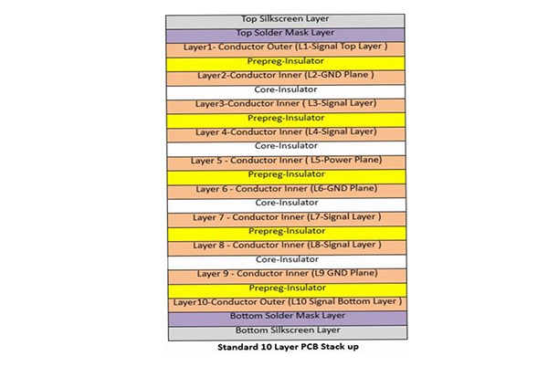
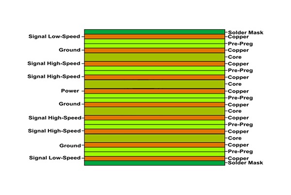
موصى به تكديس من 4 طبقات الهيكل:
الطبقة العليا: طبقة الإشارة (هيكل شريطي دقيق)
الطبقة 2: مستوى الأرض
الطبقة 3: مستوى الطاقة
الطبقة السفلية: طبقة الإشارة (هيكل شريطي)
اختيار المواد العازلة
التحديد مواد عازلة ثابتة أمر بالغ الأهمية للتحكم في المعاوقة:
- انتبه إلى الثابت العازل الكهربائي (Dk) وعامل التبديد (Df) للمادة.
- ضع في اعتبارك استقرار درجة الحرارة وخصائص التردد.
- إعطاء الأولوية للمواد منخفضة الخسارة للتطبيقات عالية التردد.
تحسين سلامة الطاقة
استراتيجية تخطيط مكثفات الفصل
تعد المكثفات الفاصلة خط الدفاع الأول للحفاظ على استقرار الطاقة:
خطة الفصل التدريجي:
- Bulk Capacitors (10-100μF): يتم وضعه عند نقاط دخول الطاقة للتعامل مع التقلبات منخفضة التردد.
- Medium Capacitors (0.1-1μF): موزعة على جميع الأطياف لتغطية نطاق الترددات المتوسطة.
- Small Capacitors (0.01-0.1μF): يوضع بالقرب من دبابيس طاقة الجهاز لقمع الضوضاء عالية التردد.
شبكة توزيع الطاقة منخفضة المقاومة (PDN)
طرق بناء شبكة توزيع طاقة منخفضة المقاومة:
- استخدم مستويات طاقة وأرضية صلبة.
- استخدم الثقوب بحكمة لتوصيل الطاقة بين الطبقات المختلفة.
- تقليل الحث المتسلسل في مسار الطاقة.
محاكاة سلامة الطاقة
استخدم أدوات مثل SPICE و HyperLynx للمحاكاة في المراحل المبكرة:
- تحديد مشاكل الضوضاء الكهربائية المحتملة.
- تحسين كمية وموضع المكثفات الفاصلة.
- تحقق من انخفاض الطاقة وهامش الضوضاء.
طرق التخفيف من تأثيرات التداخل الكهرومغناطيسي/التوافق
تحسين تقنية التأريض
التأريض السليم هو أساس تصميم EMC:
نقاط التصميم الأساسية للتأريض:
- استخدم مستويات أرضية صلبة ومتصلة.
- توفير أقصر مسار عودة للإشارات عالية التردد.
- تجنب الشقوق والفجوات في المستوى الأرضي.
تقنيات الحماية والتصفية
استخدم مجموعة من الطرق لقمع التداخل الكهرومغناطيسي:
| نوع التقنية | سيناريو التطبيق | طريقة التنفيذ |
|---|---|---|
| التدريع | حماية الدوائر الحساسة | دروع معدنية، طلاءات موصلة |
| التصفية | قمع التداخل الموجه | مرشحات EMI، حبيبات الفريت |
| الإنهاء | تقليل الانعكاسات | مقاومات مطابقة المصدر/النهاية |
استراتيجيات إدارة الحرارة
تصميم وتخطيط المبدد الحراري
- اختر مبددات حرارة ذات حجم مناسب بناءً على تبديد الطاقة.
- تأكد من وجود اتصال جيد بين المبدد الحراري وسطح الرقاقة.
- ضع في اعتبارك محاذاة اتجاه المبدد الحراري مع اتجاه تدفق الهواء.
المسارات الحرارية والوسادات الحرارية
- ترتيب مصفوفات من الثقوب الحرارية تحت المكونات المولدة للحرارة.
- Use thermal pads to increase the散热 area.
- توصيل الحرارة بشكل فعال إلى الأسطح الأرضية الداخلية.
إدارة تدفق الهواء
- ضع في اعتبارك مسارات تدفق الهواء أثناء وضع المكونات.
- ضع المكونات عالية الحرارة في مقدمة تدفق الهواء.
- تجنب المكونات الطويلة التي تعيق مسارات تدفق الهواء.
مبادئ التصميم القابل للتصنيع (DFM)
نقاط DFM الرئيسية
يمكن أن يؤدي تطبيق مبادئ التصميم الموجه نحو الإنتاجية إلى تحسين كفاءة الإنتاج والإنتاجية بشكل كبير:
بنود الفحص الحرجة لـ DFM:
- يتوافق الحد الأدنى لعرض/خلوص التتبع مع قدرات الشركة المصنعة.
- أحجام ومواقع ثقوب الحفر المُحسّنة.
- قناع لحام موحد وتصميم طباعة حريرية.
- النظر في تصميم حواف اللوحة وتصميم الألواح.
استخدام أدوات DFM المتقدمة
- استخدم أدوات مثل PCBCart DFM الفوري للتحقق من التصميم المسبق.
- احصل على تعليقات حول قابلية التصنيع في الوقت الفعلي.
- تحديد المشكلات المحتملة وتصحيحها في وقت مبكر.
اعتبارات خاصة لتصميم لوحات الدوائر المطبوعة ذات الإشارات المختلطة
التقسيم التناظري والرقمي
تعامل بشكل صحيح مع العلاقة بين الدوائر التناظرية والرقمية:
مبادئ تخطيط التقسيم:
- افصل بين مناطق الدوائر التناظرية والرقمية مادياً.
- استخدم مستويات طاقة وأرضية مستقلة.
- تنفيذ التأريض أحادي النقطة في أجهزة ADC/DAC.
استراتيجيات التأريض للإشارات المختلطة
اختر مخطط التأريض المناسب بناءً على تعقيد النظام:
مخطط مستوى أرضي واحد (مناسب للأنظمة ذات التيار الرقمي المنخفض):
- استخدم مستوى أرضي واحد ومستمر.
- السماح للتيارات العائدة التناظرية والرقمية بالانفصال بشكل طبيعي.
مخطط المستوى الأرضي المنقسم (مناسب للأنظمة ذات التيار الرقمي العالي):
- افصل بين الأراضي التناظرية والرقمية.
- قم بالتوصيل في نقطة واحدة بالقرب من مصدر الطاقة (أرضية نجمية).
- توفير مسارات تأريض واضحة للأجهزة ذات الإشارات المختلطة.
قائمة مراجعة تخطيط PCB
استخدم قائمة المراجعة التالية للتحقق النهائي بعد الانتهاء من التصميم:
- فحص سلامة الإشارة (مسارات الإشارة عالية السرعة، الإنهاء، المعاوقة)
- التحقق من سلامة الطاقة (الفصل، مقاومة PDN)
- تقييم إدارة الحرارة (تبديد الحرارة للمكونات عالية الطاقة، تدفق الهواء)
- اعتبارات EMC (التدريع، الترشيح، التأريض)
- التحقق من DFM (قيود العملية، التفاوتات المسموح بها)
- جدوى التجميع (تباعد المكونات، متطلبات اللحام)
- الوصول للاختبار وإعادة العمل (نقاط الاختبار، الوصول للمسبار)
الخاتمة
إتقان تقنيات تخطيط PCB المتقدمة هو المفتاح لتصميم أجهزة إلكترونية عالية الأداء وموثوقة للغاية. من خلال تنفيذ استراتيجيات التوجيه عالي السرعة والتحكم في المعاوقة وتحسين سلامة الطاقة وإدارة الحرارة المذكورة في هذه المقالة، يمكن للمهندسين تحسين أداء المنتج بشكل كبير مع تقليل تكاليف الإنتاج وتحسين العائد. مع تطور الأجهزة الإلكترونية نحو ترددات أعلى وأحجام أصغر، ستصبح تقنيات التخطيط المتقدمة هذه أكثر أهمية.