جدول المحتويات
1. مقدمة عن لوحات الدوائر المطبوعة والمكونات الأساسية
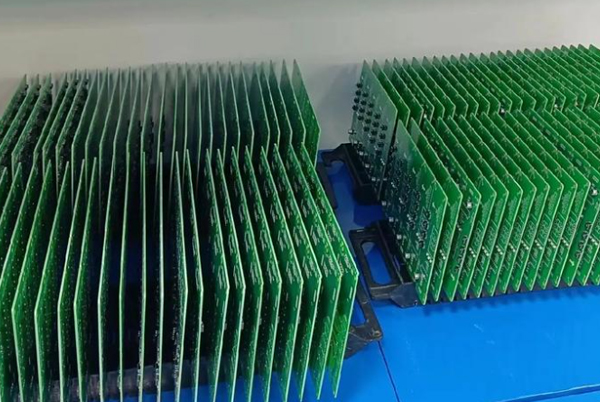
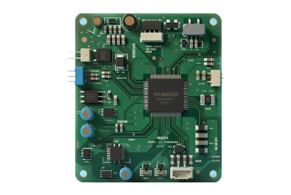
لوحات الدوائر المطبوعة (PCBs) هي مكونات أساسية في صناعة الإلكترونيات. وتشمل وظائفها الأساسية ما يلي إرسال الإشارات, الدعم المادي, توزيع الطاقةو إدارة الحرارة. تتكون لوحة الدوائر المطبوعة (PCB) من عدة عناصر متخصصة: طبقة طباعة حريرية (تراكب) لتحديد المكونات، تشطيبات الأسطح (مثل ENIG و HASL) ممرات للتوصيلات الكهربائية بين الطبقات، مكونات ثقبية (PTH) و أجهزة التثبيت السطحي (SMD)، صب النحاس (مضلع)، وسادات التخفيف الحراري, آثار الإشارات (مسار)، و وسادات، من بين ميزات مهمة أخرى.
2. نظام تصنيف PCB
2.1 التصنيف حسب مادة الركيزة
ركائز السيراميك: Utilizing materials like Alumina (Al₂O₃), Aluminum Nitride (AlN), or Silicon Carbide (SiC), these offer exceptional thermal conductivity and are designed for high-temperature environments and high-power applications.
لوحات الدوائر المطبوعة ذات النواة المعدنية (MCPCBs): بما في ذلك الركائز القائمة على الألومنيوم والنحاس، والمعروفة بقدرتها الفائقة على تبديد الحرارة، وتستخدم على نطاق واسع في الدوائر عالية الطاقة والإضاءة LED.
الركائز الورقية: مثل الدرجات FR-1 و FR-2 ، استخدم ورق الألياف كتعزيز ، مشبع بالراتنج ومغلف برقائق النحاس ، ومناسب بشكل أساسي للوحات أحادية أو ثنائية الجوانب.
الركائز المركبة: الجمع بشكل مبتكر بين خصائص مواد متعددة، على سبيل المثال، CEM-2 (راتنج إيبوكسي مع قلب من الورق وأسطح من القماش الزجاجي)، لتلبية متطلبات أداء محددة.
2.2 التصنيف حسب الخصائص الهيكلية
مركبات ثنائي الفينيل متعدد الكلور الصلبة: استخدم ركائز صلبة غير قابلة للانحناء، بما في ذلك أنواع مختلفة مثل FR-4 (إيبوكسي زجاجي)، وألواح ورقية، ومركبة، وسيراميك، وألواح ذات قلب معدني.
مركبات ثنائي الفينيل متعدد الكلور المرنة (لوحات الدوائر المطبوعة المرنة): تستخدم ركائز عازلة مرنة، مما يسمح بالانحناء واللف والطي، وهي مثالية لمساحات الأجهزة الإلكترونية المحمولة المحدودة.
مركبات ثنائي الفينيل متعدد الكلور الصلبة المرنة: دمج المناطق الصلبة والمناطق المرنة بذكاء، مما يوفر قوة هيكلية ومرونة في التركيب.
مركبات ثنائي الفينيل متعدد الكلور HDI (توصيلات عالية الكثافة): تستخدم تقنية الميكروفيات ورقائق النحاس الرقيقة للغاية لتلبية متطلبات تصغير حجم الأجهزة الإلكترونية. تشمل الهياكل توصيلات مكدسة من خطوتين، وتوصيلات متداخلة من خطوتين، وتوصيلات HDI من خطوة واحدة.
ركائز الدوائر المتكاملة: مصمم خصيصًا لتغليف الرقائق، ويوفر وظائف مهمة مثل التوصيل الكهربائي والحماية المادية والدعم الهيكلي وإدارة الحرارة.
3. تحليل متعمق لتكنولوجيا ركيزة PCB
3.1 هيكل تراص الطبقات
تتميز لوحات الدوائر المطبوعة الحديثة بتصميم متعدد الطبقات:
- اللب: رقائق مركبة من قماش الألياف الزجاجية وراتنج الإيبوكسي، مغطاة بالنحاس على كلا الجانبين.
- بريبريغ (مسبق التشريب): مركب من قماش الألياف الزجاجية والراتنج المعالج جزئيًا، مسؤول عن ربط الطبقات معًا أثناء التصفيح.
- رقائق النحاس: Divided into Electro-Deposited (ED) copper (preferred for rigid boards) and Rolled Annealed (RA) copper (used for flexible boards). Thickness is measured in ounces (OZ), e.g., 1 OZ (≈35µm).
3.2 عبر التقنيات
تصنف مسارات التوصيل بين لوحات الدوائر المطبوعة إلى ثلاثة أنواع:
- ثقب عبور: يمر عبر جميع طبقات الدائرة.
- أعمى عبر: يربط طبقة خارجية بواحدة أو أكثر من الطبقات الداخلية، ولكنه لا يمر عبر اللوحة بأكملها.
- مدفون عبر: يقع بالكامل داخل الطبقات الداخلية، ويربط بين طبقتين أو أكثر من الطبقات الداخلية دون أن يصل إلى الأسطح الخارجية.
3.3 معايير الأداء الرئيسية
المعلمات الحرارية:
- Tg (درجة حرارة التحول الزجاجي): النقطة الحرجة التي يتحول فيها الراتنج من حالة صلبة إلى حالة أكثر ليونة، مما يؤثر بشكل مباشر على مقاومة الحرارة للركيزة.
- Td (درجة حرارة التحلل): درجة الحرارة التي يفقد عندها الراتنج 5% من كتلته بسبب التحلل الحراري.
- CTE (Coefficient of Thermal Expansion): Determines dimensional stability under temperature variations. Typically X/Y: 16-18 ppm/°C, Z: 40-60 ppm/°C.
المعلمات الكهربائية:
- Dk (Dielectric Constant): Influences signal propagation speed and characteristic impedance. A lower Dk generally allows faster signal speed (V = C/√Dk).
- Df (معامل التبديد): يؤثر على سلامة الإشارة وجودتها؛ فكلما انخفض معامل التبديد، قل فقدان الإشارة.
- مقاومة السطح/الحجم: تقيس الأداء التوصيلي.
المعلمات الميكانيكية:
- قوة الانحناء وقوة التقشير
- امتصاص الماء: يؤثر على استقرار وموثوقية الركيزة. الرطوبة يمكن أن تزيد من Dk وتزيد من خطر التفريغ (“popcorning”).
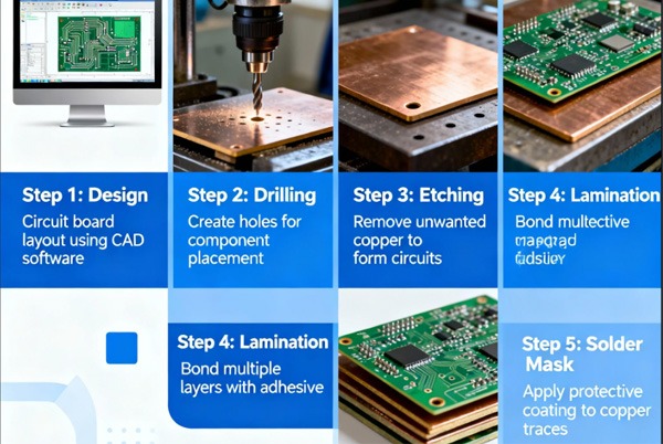
4. تدفق عملية تصنيع لوحات الدوائر المطبوعة الدقيقة
يتبع تصنيع ثنائي الفينيل متعدد الكلور تسلسلاً صارماً:
- تصوير الطبقة الداخلية → 2. تصفيح مقاوم للضوء → 3. التعرض → 4. التنمية → 5. النقش → 6. شريط مقاوم → 7. تراص الطبقات → 8. التصفيح → 9. الحفر → 10. الطلاء (PTH) → 11. طبقة خارجية مقاومة للتصفيح → 12. التعرض → 13. التنمية → 14. طلاء النقوش (النحاس/القصدير) → 15. شريط مقاوم → 16. النقش → 17. شريط من الصفيح → 18. الطباعة بالشاشة الحريرية/الطباعة الأسطورية → 19. تشطيب السطح
5. مقارنة شاملة بين معالجات تشطيب الأسطح
| تشطيب السطح | الخصائص والمزايا الرئيسية | القيود / التحديات | مستوى التكلفة | Thickness Range (µm) | مدة الصلاحية |
|---|---|---|---|---|---|
| HASL (خالية من الرصاص) | مناسب للوسادات الكبيرة والمسافات الواسعة | غير مناسب لمؤشر التنمية البشرية؛ درجة حرارة عالية؛ سطح غير مستوٍ | متوسط-عالي | 2-5 (على اللوحة) | 12 شهراً |
| HASL (قائم على الرصاص) | قوة ميكانيكية ممتازة | الاهتمام بالبيئة (محتوى الرصاص) | متوسط-عالي | 2-5 (على اللوحة) | 12 شهراً |
| OSP | عملية بسيطة، تكلفة منخفضة | غير مناسب لإعادة التدفق المتعدد؛ صعوبة الفحص | الأقل | 0.1 – 0.5 | 6 أشهر |
| ENIG (النيكل غير الكهربائي/الذهب بالغمس) | لحام موثوق به، سطح مستوٍ، مقاومة جيدة للتآكل | احتمال حدوث "بقعة سوداء" (تآكل النيكل) و"تقصف الذهب" | عالية | النيكل: 3-5 / الذهب: 0.03-0.08 | 12 شهراً |
| ENEPIG (النيكل/البلاتين/الذهب بالغمس بدون كهرباء) | تطبيقات متطورة، مقاومة فائقة للتآكل، قابلة للربط بالأسلاك | تحكم معقد في العملية، احتمال حدوث لطخات سوداء/تغير في اللون | عالية | النيكل: 2-5 / البلاديوم: 0.05-0.15 / الذهب: 0.05-0.15 | 6 أشهر |
| الفضة الغاطسة (ImAg) | سطح مستوٍ، مناسب لعمليات إعادة تدفق متعددة | يتعرض للتلف بسهولة، ويتطلب شروط تخزين صارمة | متوسط | 0.1 – 0.5 | 12 شهراً |
| قصدير الغمر (ImSn) | تسطيح جيد، قابلية للحام | خطر تشكل شعيرات القصدير، ضعف مقاومة الشيخوخة الحرارية | منخفضة | 0.8 – 1.2 | 6 أشهر |
| النيكل/الذهب الكهربائي (ذهب ناعم) | مقاومة تآكل ممتازة، موثوقية اتصال | استهلاك عالٍ للذهب، مشاكل محتملة في التصاق قناع اللحام على الذهب | الأعلى | Ni: 3-5 / Au: ≥0.05 (selective) | 12 شهراً |
| الذهب الصلب الكهربائي | مقاومة فائقة للتآكل (على سبيل المثال، للأصابع) | أعلى تكلفة، أكثر العمليات تعقيدًا | الأعلى | 0.3 - 3.0 (عند التلامس) | 12 شهراً |