The 3W principle is a key design guideline for minimizing crosstalk in PCB routing, requiring that the center-to-center spacing between adjacent signal traces be no...
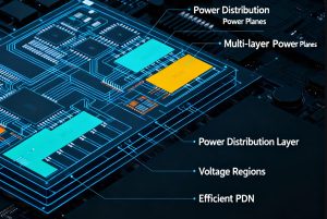
Analyzing the core elements of four-layer PCB design, including stackup selection, via parasitic parameter control, high-speed routing strategies, and power partitioning techniques, along with a...
Eighteen-layer PCB key technology-microvia design, including the definition of microvia technology, core advantages and the application value in complex multilayer boards, the three common problems...
Microvia technology for 14-layer printed circuit boards, from laser drilling specifications to solving plating defects and signal reflection problems, we offer viable solutions backed by...
PCB design is a core aspect of electronic engineering, involving the conversion of circuit schematics into actual production-ready printed circuit board layouts, requiring comprehensive consideration...
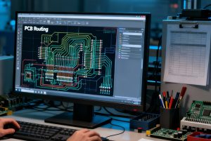
Altium Designer is a powerful all-round PCB design tool, covering the schematic design to PCB layout of the full range of processes and other functions,...
n the manufacture of electronic products, multi-layer PCB (printed circuit board) design and production is an indispensable key link, patchwork design (Panelization) is a PCB...