Das 3W-Prinzip ist eine wichtige Designrichtlinie zur Minimierung von Übersprechen beim PCB-Routing, wonach der Abstand zwischen den Mittelpunkten benachbarter Signalleitungen nicht ...
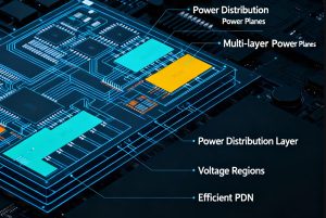
Analyse der Kernelemente des vierlagigen Leiterplattendesigns, einschließlich der Auswahl des Lagenaufbaus, der Steuerung parasitärer Parameter, Strategien für das Hochgeschwindigkeits-Routing und Techniken zur Leistungsaufteilung, zusammen mit einem...
Achtzehnschichtige Leiterplatten-Schlüsseltechnologie – Microvia-Design, einschließlich der Definition der Microvia-Technologie, der Kernvorteile und des Anwendungswerts in komplexen Mehrschichtplatinen, der drei häufig auftretenden Probleme...
Microvia-Technologie im 14-Lagen-Leiterplatten-Design
Microvia-Technologie für 14-lagige Leiterplatten: Von den Spezifikationen für das Laserbohren bis hin zur Behebung von Beschichtungsfehlern und Signalreflexionsproblemen bieten wir praktikable Lösungen, die sich auf ... stützen.
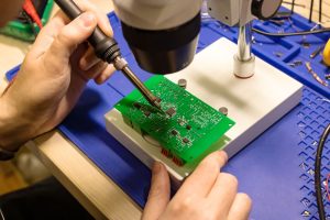
Das PCB-Design ist ein zentraler Aspekt der Elektrotechnik, bei dem Schaltpläne in tatsächlich produktionsreife Leiterplattenlayouts umgewandelt werden, was eine umfassende Betrachtung erfordert...
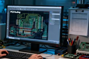
Altium Designer ist ein leistungsstarkes Allround-Tool für das PCB-Design, das alle Prozesse und Funktionen vom Schaltplan-Design bis zum PCB-Layout abdeckt...
Bei der Herstellung elektronischer Produkte ist die Entwicklung und Produktion mehrschichtiger Leiterplatten (PCB) ein unverzichtbarer Schlüsselprozess. Das Patchwork-Design (Panelization) ist eine PCB...